Co-Packaged Optics Step Into the Spotlight

Optical interconnects in the data center took center stage at NVIDIA’s GTC 2025 conference in March when Jensen Huang announced two network switches incorporating co-packaged optics (CPO), which combine photonics and electronics in a single package for higher performance and efficiency. Unveiled during Jensen’s keynote, the Quantum-X (2H 2025) and Spectrum-X (2H 2026) deliver 1.6T and 3.2T silicon photonics co-packaged optics chips that eliminate the need for pluggable transceiver modules.
Why is this so significant?
According to Jensen, it’s all about reducing energy consumption to scale systems effectively and add more GPUs. “Energy is our most important commodity,” he said. Each GPU requires six pluggable electrical-to-fiber transceivers, with each consuming 30 watts of power. According to some back-of-the-envelope math, scaling up to a million GPUs would consume approximately 180MW—an unsustainable figure for large-scale systems.
The buzz around co-packaged optics continued at OFC 2025, where startups and major players alike showcased the progress of optical interconnects. This, of course, comes as no surprise to us. Ayar Labs recognized early on the potential for co-packaged optics, which positioned us to drive the adoption of optical solutions in AI (artificial intelligence) applications.
Today, CPO is the most critical technology for scaling AI systems, as its advantages for scale-out and scale-up networks are becoming increasingly clear. Both architectures offer unique approaches to meet the demands of these systems.
- Scale-out architectures interconnect separate compute clusters in a data center by using standard networking technologies like InfiniBand or Ethernet. These networks often feature tapered bandwidth and are designed to handle communications across longer distances within the data center infrastructure.
- Scale-up architectures operate within a compute cluster, aiming to maximize intra-cluster communication bandwidth and minimize latency among tightly packed computing resources, such as GPUs. Scale-up networks are currently confined to a rack due to the reach limit of electrical interconnects, and they require advanced interconnect solutions like in-package optical I/O to expand to multi-rack configurations.
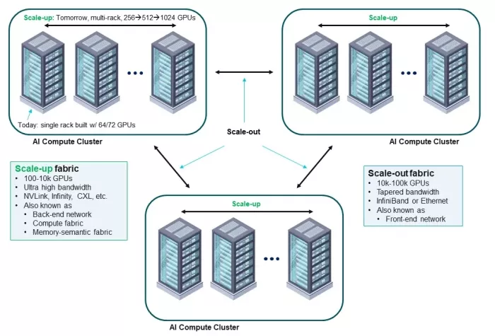
Figure 1: Scale-out and scale-up networks in AI compute clusters.
While scale-out is easier to implement and serves as an initial entry point for adopting optical solutions, Ayar Labs sees scale-up as the bigger challenge—and the bigger market opportunity. Scale-up requires at least 10x more bandwidth and a 10x reduction in latency, which necessitates integrating the optical chiplet directly into the GPU package.
As our co-founder and CTO, Vladimir Stojanovich, likes to say, “The road to scale-up leads through scale-out.” By first focusing on scale-out solutions, our industry is developing the CPO ecosystem needed for mass production. This is important because these scale-up fabrics are essential to improving AI profitability.
To understand today’s co-packaged optics landscape, let’s take a step back and look at the broader picture of how it has advanced over the last several years.
The Evolution of Co-Packaged Optics
The industry’s perception and implementation of co-packaged optics have undergone significant changes since the first products using ASICs co-packaged with optics were announced in 2021. Historically, co-packaged optics modules had their own package substrate and were assembled with a switch on a large interposer board versus in the same package as the switch SoC (system on chip) (Broadcom, as an example). Optical I/O, on the other hand, differentiated itself early by integrating the optical engine chiplet within the same package as the main SoC.
Fast forward to today, and co-packaged optics integration has advanced significantly. As we see with NVIDIA’s recent implementations, co-packaging the optical engine and switch silicon within the same SoC represents an evolutionary leap in physical form factors and technology. As a result, the distinction between scale-out switch solutions and scale-up GPU-to-GPU connections is fading as both approaches converge on similar co-packaged architectures.
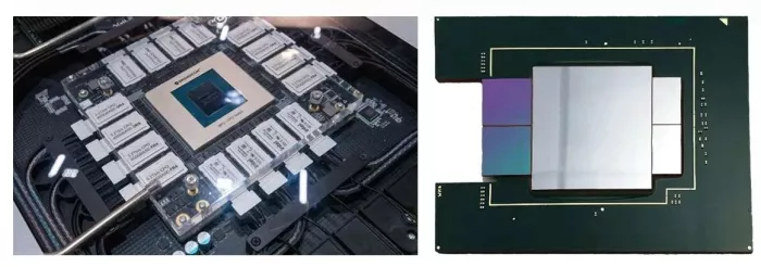
Figure 2: Broadcom’s co-packaged optics shown at OCP Summit 2022 (left) and Ayar Labs’ co-packaged optics with two TeraPHY™ optical engine chiplets and a customer FPGA within the same SoC package (right).
Advancements in scale-out networks are now creating the ecosystems necessary for optics to also address scale-up networks more efficiently. This is set to enable more seamless GPU-to-GPU connections in order to support the computing demands of large-scale AI models. This is where optical interconnects—particularly co-packaged optics and Ayar Labs’ optical I/O—shine.
The Importance of Optical Interconnects in AI Infrastructure
Optical interconnects offer increased reach, reduced power consumption, higher bandwidth density, lower latency, and higher radix than electrical interconnects. These key factors become bottlenecks when building clusters larger than a single rack of GPUs using electrical interconnects. That’s why there’s been so much interest in optical interconnects as AI development continues to accelerate. However, because AI needs more computing power than ever before, new solutions are required to tackle these scaling challenges.
The Yole Group writes that in-package optics are a key enabler for AI and machine learning (ML). As Dr. Martin Vallo, Yole’s senior technology & market analyst for photonics, explains:
“Applications such as AI/ML frequently need to move data rapidly from one chip to another or one board to another. Consequently, the computing chips need more communication, either through a larger number of pads or very high speed in a single pad. Additionally, data movement power is the primary driver of power increases in server chips.”
Ayar Labs Launches First UCIe Optical Chiplet for AI Scale-Up
Leading the co-packaged optics news blitz at OFC, we announced the world’s first UCIe (Universal Chiplet Interconnect Express) optical chiplet designed for AI scale-up architectures. Capable of achieving 8 Tbps bandwidth, this breakthrough represents Ayar Labs’ continued leadership in the CPO category by building on our expertise in developing optical engines featuring microring resonators and multi-wavelength light sources.
At the heart of this innovation is our TeraPHY™ optical I/O chiplet, powered by the SuperNova™ external light source, a 16-wavelength solution that enables unmatched bandwidth density and scalability. Using a microring-based optical engine, Ayar Labs uniquely positions itself as a pioneer in the integration of optics and silicon, embodying the next evolution of efficient scale-up networks tailored for large-scale AI models.
This UCIe optical chiplet allows GPUs and other accelerators to communicate across distances ranging from millimeters to kilometers, while effectively functioning as a single, giant GPU. Integrating a UCIe interface means this solution delivers high performance and efficiency while also enabling interoperability among chiplets from different vendors. Adhering to the UCIe standard fosters a more accessible and cost-effective ecosystem, paving the way for broader adoption of advanced optical technologies.
Key technical details of Ayar Labs’ UCIe optical chiplet include:
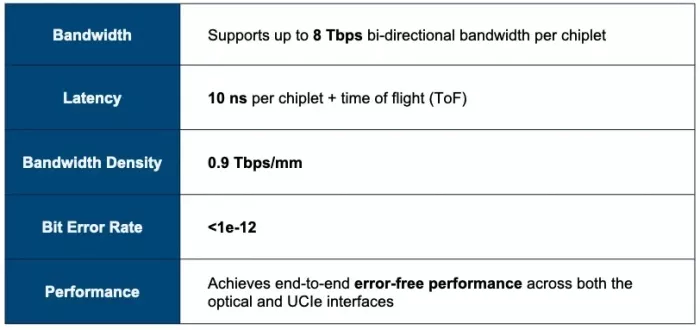
Figure 3: Ayar Labs UCIe optical chiplet specifications.
Not only does Ayar Labs deliver real working silicon, but it also led the team that designed the optics in the world’s first processor to communicate using light. Today, the company holds 200+ patents in photonics and related fields as it continues to set benchmarks in optical I/O innovation.
Dr. Debendra Das Sharma, chair of the UCIe Consortium, remarked:
“The advancement of the UCIe standard marks significant progress toward creating more integrated and efficient AI infrastructure thanks to an ecosystem of interoperable chiplets. By fostering interoperability and collaboration among vendors, UCIe provides the foundation to meet the growing demands for greater bandwidth and energy efficiency. It is incredibly encouraging to see Ayar Labs contribute to this momentum with this UCIe optical I/O chiplet.”
By leveraging a microring resonator-based optical engine, Ayar Labs’ co-packaged optics solution—consisting of the TeraPHY optical I/O chiplet and SuperNova external light source—is setting the stage for AI architectures that demand unparalleled scalability, energy efficiency, and bandwidth density.
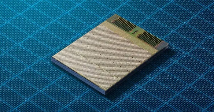
Figure 4: Ayar Labs UCIe optical chiplet was announced during OFC 2025. Capable of achieving 8 Tbps bandwidth, the TeraPHY™ optical I/O chiplet is powered by Ayar Labs’ 16-wavelength SuperNova™ external light source.
The Future of Co-Packaged Optics at Scale
To support broader adoption, we are actively collaborating with OSATs and other key industry players to establish a strong ecosystem for high-volume manufacturing. These partnerships are playing an important role in the deployment of optical I/O solutions, helping us build and integrate with a high-volume, global semiconductor supply chain. We are also focused on fostering industry-wide standardization, making it easier to connect our optical I/O chiplets with other chips inside one package. Ultimately, these collaborations and efforts are vital for proving reliability and quality at scale.
Learn how Ayar Labs is transforming next-generation AI systems with co-packaged optics at https://ayarlabs.com/artificial-intelligence.
Related Chiplet
- DPIQ Tx PICs
- IMDD Tx PICs
- Near-Packaged Optics (NPO) Chiplet Solution
- High Performance Droplet
- Interconnect Chiplet
Related Blogs
- What are Chiplets and how they Assemble Into the Most Advanced SoCs
- Overcoming interconnect obstacles with co-packaged optics (CPO)
- The Future of Chiplet Reliability
- Prototyping Chiplets from the Desktop!
Latest Blogs
- From horsepower to high-performance compute: automotive chiplets take the leap towards autonomous edge computing
- Designing the Future We Can Verify: A Vision for Multi-Die Design, STCO, and Trustworthy AI
- Wafer-Scale vs. Chiplets: The new war? - Part 2: Two Paths, One Wall
- Wafer-Scale vs. Chiplets: The new war?
- Chiplets 101: An Arteris Guide to Multi-Die Architecture