Cadence Sets the Gold Standard for UCIe Connectivity at Chiplet Summit '24

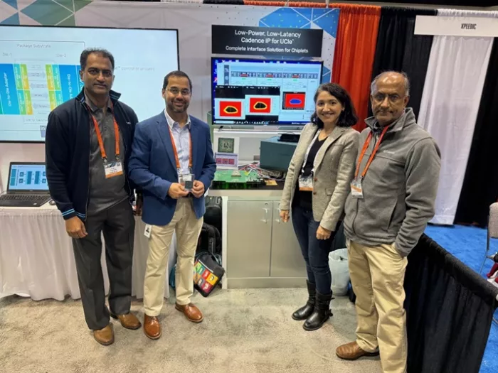
Cadence demonstrated multiple IP for die-to-die connectivity at Chiplet Summit 2024. Conference attendees discussed their chiplet and multi-die design needs with our experts and learned how Cadence’s IP can support them in achieving their system needs with optimum PPA targets. Our UCIeTM IP silicon demo created a buzz with its extensive testing.
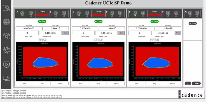
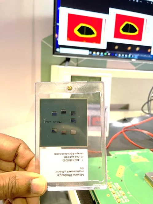
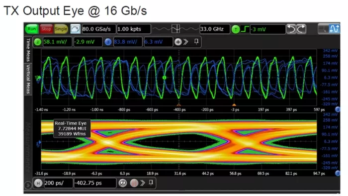
Cadence unveiled the first silicon of its UCIe IP with organic package at the summit. In an industry first, Cadence proved successful bring-up and data traffic across the complete range of interconnect distances—short-, medium-, and long-reach channels—operating at 16GT/s speeds with wide open data eyes. The stringent UCIe requirements must be met across all interconnect distances per the standard requirements. Cadence was the only IP provider that demonstrated successful 5mm, 15mm, and 25mm long-reach UCIe operation at the summit, setting the gold standard with its thorough measurement and reporting.
The first-pass silicon that features die-to-die connectivity at various distances is allowing designers at Cadence to gather valuable information, as well as highlighting the quality of our IP to the end-users of these solutions. The design is a testament to Cadence’s commitment to extensive testing and analysis, while the wide-open data eyes for all three channel reach links prove Cadence’s ability to design a high-performance IP that meets and exceeds specifications.
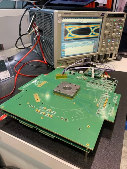
The test-chip includes seven chiplets, each with two UCIe PHY blocks.
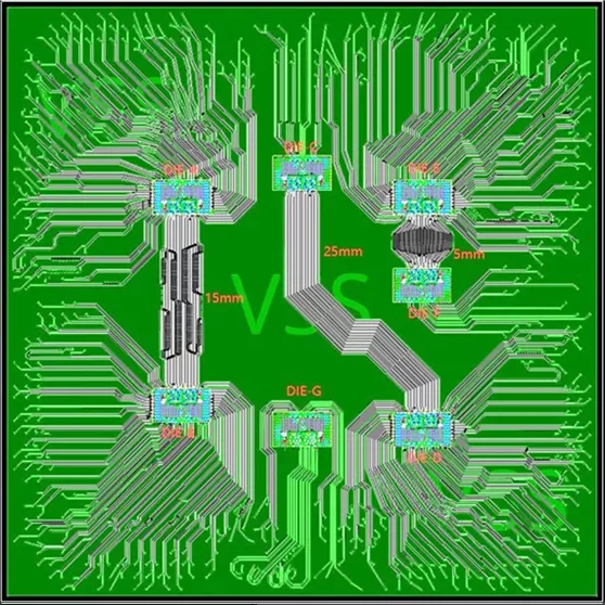
Six of the chiplets are placed in three pairs, at 5mm, 15mm, and 25mm interconnect distances, respectively. The 25mm routes also have turns that called for careful package design to minimize reflections and discontinuity and allow measurement of those effects. A seventh, standalone chiplet, is accessed through packaged pins and the high-speed transmit data and clocks are brought to an oscilloscope for viewing the eye-diagram in real time. Such measurement of a die-to-die interconnect on an oscilloscope was another novel addition by the Cadence team.
The first-pass silicon success for our UCIe IP was welcome news but not surprising, as the Cadence design team has gained significant expertise over six years, designing three generations of the proprietary UltraLink die-to-die interconnect solution, which went through multiple successful test chips targeting various PDK nodes and design flavors and is now in high-volume production with multiple customers. The UCIe IP design was built using that experience and expertise, delivering exceptional performance and PPA metrics.
Our demos attracted a lot of attention at the Chiplet Summit with many key partners and customers, who stopped by to understand Cadence’s UCIe offering and talking to our experts. There was a high degree of appreciation for the standard Cadence is setting in testing die-to-die interconnect IP that is becoming increasingly ubiquitous with many players, big and small, both on the design and the use side.
The measurements showed excellent characteristics. The eye diagrams were clean across frequencies of operation (16GT/s, 12GT/s, 8GT/s and 4GT/s), and link training and bring-up went smoothly. The bring up included complete link training and self-calibration, without requiring any manual overriding of calibration loops or “tweaking”, demonstrating a fully capable and self-training PHY. The intuitive layout of Cadence’s demonstration interface allowed visitors to readily understand our data and fostered meaningful discussions.
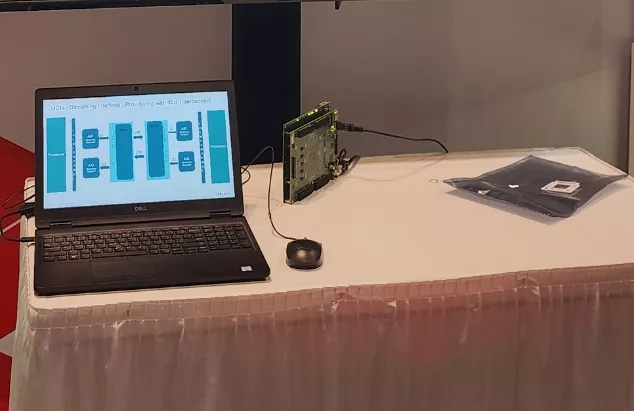
While the silicon sample showed the physical PHY, an FPGA prototyping demo displayed the controller and logical PHY. Using a 256bit parallel interface, it can prototype a 16bit UCIe interface allowing users to build up their stack on both sides of the interface, even before the UCIe SerDes and package interconnects are completed. This co-development will reduce time to market and allow users to optimize their system for use with the UCIe IP very early in the design cycle. In the demo, the prototype went through reset, link training state machine (LTSM), followed by mission mode traffic, with the option to inject and observe errors.
If you missed our demos or would like to know more about how Cadence’s IP for UCIe can support your chiplet and multi-die designs, please contact me at bmayank@cadence.com. At Cadence, we are more than happy to talk about UCIe and all the possibilities it opens up for our customers in the golden age of chiplets, disaggregation, and heterogenous integration.
Related Chiplet
- DPIQ Tx PICs
- IMDD Tx PICs
- Near-Packaged Optics (NPO) Chiplet Solution
- High Performance Droplet
- Interconnect Chiplet
Related Blogs
- UCIe and Automotive Electronics: Pioneering the Chiplet Revolution
- AI System Connectivity for UCIe and Chiplet Interfaces Demand Escalating Bandwidth Needs
- Advancing Die-to-Die Connectivity: The Next-Generation UCIe IP Subsystem
- Advancing Die-to-Die Connectivity: The Next-Generation UCIe IP Subsystem
Latest Blogs
- Accelerating Chiplet Innovation with a New Partner Ecosystem
- Accelerating Multi-Die Innovation: How Synopsys and Samsung are Shaping Chip Design
- Six critical trends reshaping 3D IC design in 2026 and beyond
- AI Energy Gap and Chiplets: Why Data Movement Matters
- The Economies of Disaggregation: Why the Future is a System-of-Chiplets