Ayar Labs Optical Connectivity for AI Compute Fabrics
I’m often asked about the origins of Ayar Labs and how we find ourselves at the forefront of large-scale AI computing’s shift to optical connectivity. Our journey has been a mix of deep technical insights, bold bets on new architectural approaches, and perhaps a dash of naïveté to pursue first-principles solutions long before they became mainstream.
Today, the industry is at an inflection point, primed to adopt optical connectivity as the only viable solution to scale performance, power efficiency, and economics in large-scale AI and high-performance computing (HPC) systems. Within the past few years we have seen the advancement of networking performance through the rise of co-packaged optics (CPO), integrating photonic and electrical components in a single package. Within the next few years, we’ll see the proliferation of optical component integration, including chip-to-chip optical interconnects, deliver the promise of AI by eliminating the data bottleneck limitations of traditional copper and electrical interconnects. I’d like to briefly reflect on how we arrived at this critical moment—and share a vision for the future we’re actively shaping.
The Connectivity Bottleneck
In 2010 my co-founders and I were academic researchers at the Massachusetts Institute of Technology (MIT); University of California, Berkeley; and University of Colorado Boulder. During those early years, we examined trends in CMOS transistor density, memory capacity, and network bandwidth. A widening gap became clear: compute power was rapidly outpacing memory and network performance. At the heart of this bottleneck were the fundamental limits of electrical interconnects.
We realized that the bandwidth-distance problem historically solved by optics in long-haul communications would impact chip-to-chip architectures. Traditional electrical links would no longer deliver the density, efficiency, or latency needed for future compute fabrics. Recognizing this early on, we embraced a new approach and pioneered the use of optical interconnects at a time when such an approach was still far from mainstream.
Inventing Optical Connectivity for Compute Fabrics
This insight drove us to develop integrated photonics technologies specifically tailored for computing applications, not just networking. We focused on developing new silicon photonic devices, integrated electronic-photonic circuits, and external multi-wavelength laser sources. Our groundbreaking work culminated in the world’s first microprocessor to communicate optically with memory and marked an important milestone in our journey to revolutionizing interconnects for data movement.
Motivated by this breakthrough, we founded Ayar Labs in 2015, intent on bringing these innovations from academia into real-world systems. Our mission was clear: solve the foundational connectivity bottleneck in computing systems using a new generation of electronic/photonic integration and architectures.
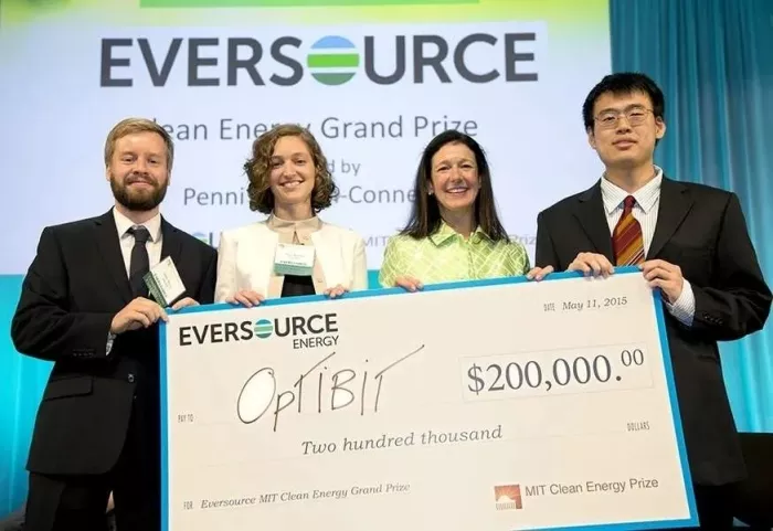
Figure 1: Co-founders Mark Wade (left), Alex Wright (second left), and Chen Sun (right) took home both grand prizes from the 2015 MIT Clean Energy Prize under the team name Optibit.
Early Challenges and Opportunities
In our early years (2015–2018), the ecosystem wasn’t yet ready for our innovations. We faced gaps in manufacturing, assembly, and test infrastructure, and most importantly, lacked a high-volume market application to motivate industry collaboration. However, we identified several key developments that would define our path forward:
- Chipletization: The end of Dennard scaling and advanced node yield challenges drove major players like AMD, Intel, and others toward chiplet architectures, creating a pathway for our optical chiplet innovation.
- Manufacturing Advances: Foundries such as GlobalFoundries, Intel Foundry, and TSMC advanced their silicon photonics capabilities, aligning closely with our integration goals.
- Rise of AI Workloads: The explosion of accelerated computing for AI (e.g., Google TPUs, custom silicon startups) suggested a shift toward distributed, connectivity-intensive architectures.
Recognizing these trends, we made a bold bet in our 2018 Series A: that large-scale AI systems would emerge as the primary data center workload, and optical I/O would be critical for their scalability and economics. The subsequent arrival of transformer architectures and ChatGPT in late 2022 validated our prediction.
Building Strategic Partnerships for High-Volume Deployment
To turn our vision into reality, we cultivated strategic relationships across the ecosystem:
- Manufacturing & Assembly: Deep partnerships with GlobalFoundries, Intel Foundry Services, and TSMC.
- Compute Leaders: Strategic alliances and investments from NVIDIA, AMD, and Intel.
- Standards & Ecosystem: Supporting industry standards like Universal Chiplet Interconnect Express (UCIe) and fabric protocols such as Ultra Accelerator Link (UALink) to foster broad adoption.
These collaborations are now accelerating the transition of optical I/O into high-volume products for GPU fabrics, accelerators, and memory-semantic switches.
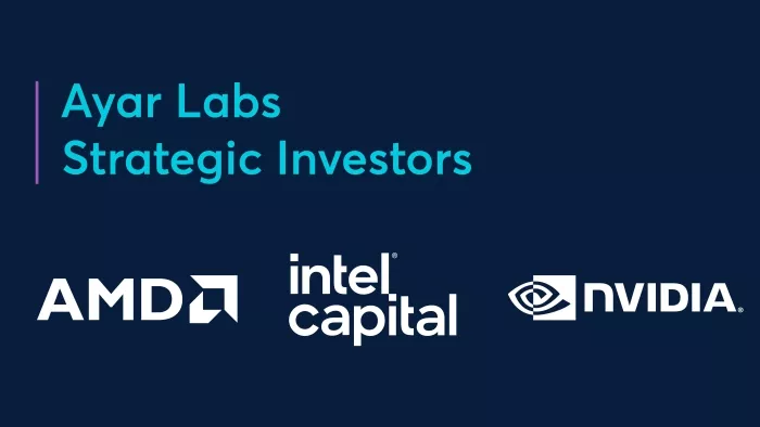
Figure 2: Ayar Labs’ strategic partners include AMD, Intel Capital, and NVIDIA.
The Path Forward: Optical Connectivity’s Impact on AI Systems
At Ayar Labs, we are deeply driven by the scale of impact that optical connectivity can deliver for the most critical technology challenge of our era: large-scale AI. While challenges remain, our partners and the broader industry ecosystem are now rapidly converging and accelerating toward a new era of computing powered by optical connectivity, notably:
- Foundry processes (e.g., GF Fotonix, TSMC COUPE) are nearing high-volume manufacturing production readiness.
- Tier-1 OSATs are building scalable assembly and packaging processes.
- Laser suppliers are readying volume production for external laser sources.
- AI-focused compute giants (NVIDIA, AMD, Intel) are driving direct demand for optical connectivity.
As the ecosystem prepares for the market shift to optical solutions, we see the adoption coming in phases over the coming years:
- Data Center Networks: Initially, optical connectivity will optimize scale-out switching fabrics (Ethernet, InfiniBand), significantly improving overall data center power efficiency.
- GPU/Accelerator Fabrics: Ayar Labs’ optical interconnect technology will revolutionize scale-up connectivity for GPU clusters, expanding the domain size from today’s ~64 GPUs to hundreds or even thousands, fundamentally enhancing AI system performance and economics.
- Memory & Storage Integration: Long term, optical connectivity will extend directly into main memory and storage appliances, fully realizing our initial vision of optically connected compute architectures.
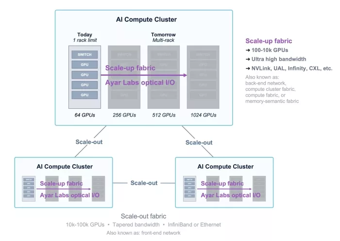
Figure 3: Ayar Labs’ optical I/O solution is ideally suited for next-gen AI scale-up architectures.
The Ayar Labs journey has been extraordinary and while we recognize how unique it is to be a part of an industry revolution, we also embrace the opportunity to continue to lead optical connectivity’s impact on large-scale AI systems.
Related Chiplet
- Integrated voltage regulator (IVR) chiplet
- High-performance connectivity chiplets
- eFPGA Chiplet
- DPIQ Tx PICs
- IMDD Tx PICs
Related Blogs
- Let’s Get Serious: TeraPHY™ Optical Engine Passes the Test for AI Scale-Up at Volume
- The Future of Chip Connectivity: UCIe and Optical I/O FAQs Explained
- The Future of Chip Connectivity: UCIe and Optical I/O FAQs Explained
- Breaking Through Bottlenecks: Executives from AMD, Ayar Labs, Cerebras, and Microsoft, Discuss the Future of AI Infrastructure with Optical I/O
Latest Blogs
- The Bottleneck Isn’t Compute. It’s Getting the Chip Built!
- How Intel Foundry Packaging Technologies Redefine AI and HPC Scalability Limits at ECTC 2026
- From complexity to simplicity: Scaling and future-proofing chiplets with AMBA®︎ CHI C2C property negotiation
- High-Speed Heterogeneous Integration with Multiphysics Analysis for TSMC SoW-X
- Chiplet Realization Beyond the Package: Why the Next AI Bottleneck Moves to the Interposer-to-PCB Boundary