Breaking Through Bottlenecks: Executives from AMD, Ayar Labs, Cerebras, and Microsoft, Discuss the Future of AI Infrastructure with Optical I/O

The semiconductor industry is buzzing with discussions around the challenges of scaling AI infrastructure. One topic of particular focus is the limitations of copper interconnects and the promising potential of silicon photonics, optical I/O in particular, to meet growing bandwidth demands.
How can the industry identify and eliminate these bottlenecks to support increasingly complex workloads? What is required for scalable, flexible optical I/O implementation to become a reality? And how can industry standards help reduce costs and increase the adoption of optical I/O?
Recently, a group of industry leaders from AMD, Ayar Labs, Cerebras Systems, and Microsoft Azure came together to address these pressing questions.
For starters, why are copper interconnects reaching their limit?
Copper interconnects have a fundamental bandwidth-reach trade-off: the higher the bandwidth, the shorter the reach. For example, 200 Gbps can stretch across a meter per line today, but you simply cannot extend that to 400 Gbps over a meter or 200 Gbps over two meters. This constraint effectively limits the scaling of AI systems to a single rack.
Vladimir Stojanovic, Ayar Labs’ chief technology officer and co-founder, explains that this kind of trade-off is what is currently affecting the scaling of AI systems.
“Doubling of bandwidth on any kind of medium is bound to run out of steam and hit the basic physics limitations at some point. Copper has had a very long run—almost three decades. My view on it is that we should limit anything we do with copper to a rack level, at least on the high-bandwidth scale-up domain. Because the biggest problem currently in the scale-up domain is being able to free yourself from the shackles of copper within a rack.”
What are the most important I/O architecture changes necessary to enable generative AI (GenAI) in the cloud?
Nidhi Chappell, VP/GM of Azure AI and HPC Platform at Microsoft, emphasizes the need for increased I/O bandwidth and reliability.
“We need a lot more I/O bandwidth, and we need it very reliably. People forget that these workloads actually don’t tolerate failures very well, especially I/O failures.” She added, “Because we need so much bandwidth, we end up having super dense rack designs, which is good from a power density point of view. But it has its own challenges. The field is ripe for something that can provide bandwidth, reliability, and scalability at a low cost point. Silicon photonics is one of the technologies that definitely has promise.”
How have the requirements for inference and training workloads changed in the last few years, and how does that affect I/O requirements?
Traditionally, inference workloads were expected to become simpler over time. However, contrary to these expectations, they have become more complex.
Jean-Philippe Fricker, chief systems architect at Cerebras Systems, notes, “There is a new trend in generative AI inference to let the network ‘think about it’ before answering. The inference workloads we’ve been accustomed to being super-fast and not requiring a lot of bandwidth are evolving and becoming more like training.”
As a result, the architecture needed for inference is becoming increasingly similar to what is used for training, though key differences remain. This convergence necessitates enhanced I/O capabilities to meet the bandwidth-intensive data processing demands of modern inference tasks and optimize throughput and latency.
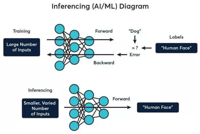
Figure 1. Inferencing is the process of using a trained machine learning model to make predictions or decisions based on new, unseen data.
There is a consensus that co-packaged optics (CPO) spanning the rack within a system would be beneficial. So, why haven’t we widely implemented this technology already?
Robert Hormuth, VP of Architecture and Strategy at AMD, sees several issues.
“The industry has been attempting to stay in copper at all costs due to the optical cost, power, and reliability. But another issue is alignment to SoC (system on a chip) architectures. GPUs and CPUs have very wide buses running very slowly, comparatively speaking, because they want to operate on data, not just pass it along. How do you get that out of the chip without a bunch of cost and power and latency?”
Hormuth argues that for CPO to be widely adopted, it “needs to align with SoC plumbing.” He highlights the important distinctions between load/store operations, memory semantic fabrics, and networking. The latencies of Ayar Labs’ optical I/O chiplets are on the order of ten nanoseconds, and the raw bit error rates (BER) are better than 1e-12.
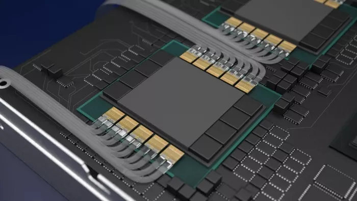
Figure 2. Ayar Labs’ optical I/O technology integrated into a multi-chip compute node.
Dense wavelength division multiplexing (DWDM) offers more lanes, making it a much better match to the wider buses that Hormuth references. This alignment reduces the need for “gearboxing” because optical I/O chiplets use die-to-die interfaces. For instance, UCIe (Universal Chiplet Interconnect Express) is a wide parallel standard that is much closer to a high bandwidth memory (HBM) interface in terms of pin density compared to SerDes.
How long will it take before lasers are reliable enough for optical interconnects to be mainstream?
“Lasers have a lot of promise, but they take more power today. Reliability is also a factor,” Chappell explains. “At some point, they will be the answer, but there is still room for growth.”
Ayar Labs addresses these issues by moving the laser outside the package, incorporating multi-wavelength designs, and balancing system architecture to support memory semantic fabrics. This lowers power consumption per wavelength, significantly improving the reliability of the external laser, as well as its placement and cooling.
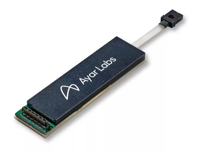
Figure 3. Ayar Labs’ SuperNova™ remote light source is an example of an external laser source (ELS).
What industry standards will be developed for optics, and how will they affect cost?
Chappell underscores the importance of standardization: “This workload is very volatile. A workload that is changing very quickly and a vendor-specific implementation is a complete recipe for disaster. You cannot have ten bespoke designs. For anybody to get to scale implementation that can be scalable in multiple scenarios, we need to get to a standard that enables us to go and test different implementations.”
Hormuth adds, “To really get the optics down, we’ve got to think about how we drive industry standards to drive volume. Volume drives everything.”
However, there are differing opinions on what these standards should entail and how many should be developed.
The biggest question in Hormuth’s mind: “Is it one-size-fits-all optics? Or is there optics for a packet world, and optics for the load store world? Just think about the two approaches of the coarse wavelength division multiplexing (CWDM) and PAM4 versus the dense wavelength division multiplexing and NRZ—drastically different. So, do we end up with two different sets of optical standards, or is it going to be one size fits all?”
Despite these differing views, industry experts agree that standards are vital to the growth and success of optical I/O. Regardless of the specific technology, standardizing key aspects such as the die-to-die interface and the optical connector is essential. These standards influence packaging and integration into the environment, ultimately boosting volume in these applications.
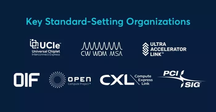
Figure 4. Ayar Labs is a member of these key standard-setting organizations, which are vital to the growth and success of optical I/O.
When will we see silicon photonics first deployed in AI systems?
The industry consensus is that silicon photonics will be deployed within the next few years. Chappell states, “I think it’s a couple of years out. It’s not ten. There are lots of smart people working on it. There is definitely a lot of need in the ecosystem.”
Hormuth agrees, predicting: “I think co-packaged optics is more aligned to top-of-rack switching and switch silicon. That’s probably the first volume intercept. We’ll be there when Microsoft tells us to be ready.”
Meanwhile, the task ahead for Ayar Labs involves ramping up the entire manufacturing ecosystem to get to tens of millions of chiplets a year to meet these future demands.
Hormuth concludes, “We’ve got to get to volume, economies of scale, and standards. That’s the recipe for success.”
To learn more about strategies that will shape the future of AI infrastructure, including Ayar Labs’ optical I/O solution, watch the on-demand webinar, https://ayarlabs.com/resources/unlocking-the-future-of-ai-infrastructure/.
Related Chiplet
- DPIQ Tx PICs
- IMDD Tx PICs
- Near-Packaged Optics (NPO) Chiplet Solution
- High Performance Droplet
- Interconnect Chiplet
Related Blogs
- Intel® Shows OCI Optical I/O Chiplet Co-packaged with CPU at OFC2024, Targeting Explosive AI Scaling
- Alphawave Semi Tapes Out Industry-First, Multi-Protocol I/O Connectivity Chiplet for HPC and AI Infrastructure
- Samsung Foundry Partners with Arm, ADTechnology and Rebellions to Develop an Innovative AI CPU Chiplet Platform Ideal for Modern AI Datacenters
- The Future of Chip Connectivity: UCIe and Optical I/O FAQs Explained
Latest Blogs
- Simulation Solutions for the Structural Integrity of Chip Packages
- Overcoming interconnect obstacles with co-packaged optics (CPO)
- Chiplets: 8 best practices for engineering multi-die designs
- Demystifying 3D ICs: A practical framework for heterogeneous integration
- Accelerating Next-Generation EMIB-T Packaging: A Collaboration Between Synopsys and Intel Foundry