Let’s Get Serious: TeraPHY™ Optical Engine Passes the Test for AI Scale-Up at Volume
As we’ve discussed previously, the increasing scale of AI workloads is pushing the boundaries of traditional copper interconnects. To enable next-generation performance, today’s optical I/O components must not only push bandwidth—they must also withstand the most rigorous real-world challenges. That’s why Ayar Labs recently put its TeraPHY™ optical I/O chiplet through a battery of engineering validation and thermal tests. Spoiler alert: It passed with flying colors.
The TeraPHY optical engine is the industry’s first Universal Chiplet Interconnect Express (UCIe) optical interconnect chiplet that can deliver 8 Tbps of bandwidth. Built to maximize AI scale-up architecture performance and efficiency, it reduces latency and power consumption while overcoming the bandwidth and reach limitations of traditional copper interconnects. Recent testing found it performs as expected at temperature change rates as high as 800 degrees C/s, with bit error rate (BER) staying under the spec across a range of circumstances.
This type of in-depth validation—including wafer sort, engineering validation test (EVT), and design validation test (DVT)—is extremely important as optical I/O products move beyond demos to manufacturing at scale. These tests assess the viability, stability, and robustness of optical interconnects in co-packaged optics (CPO) compute and switch scenarios. They reveal design flaws and areas where the design falls short of the model, which must be addressed in order to successfully ramp manufacturing.
As AI scale-up drives increased demand for co-packaged optical engines, vendors must push past prototypes and demos and get serious about testing their solutions at scale and in the real world.
8 Tbps of Bandwidth, Built for Compatibility
The TeraPHY optical I/O chiplet has matured significantly over three generations. First was a 2 Tbps chiplet built mainly for multi-chip package (MCP) integration and demonstration. Then a 4 Tbps version that went through extensive wafer-level sort testing (with the world’s first electro-optic wafer sort capability development), bring-up, EVT, DVT, all the way through the MCP and system integration stage. The 8 Tbps TeraPHY has gone through further improved electro-optic wafer sort testing (and benefits from what we learned with the last generation), as well as extensive engineering validation and test characterizations.
The chip is both the first implementation of a UCIe optical retimer and the first demonstration of 16-wavelength microring-based links. There is some skepticism in the industry about using microring resonators in CPO for high-volume GPUs. Ayar Labs has been working on this technology for years, and these results show that, without a doubt, we have the technology to control and operate these microrings in the system application conditions at the link levels, margins, and quantities needed for high-volume manufacturing.
With the introduction of the 3.0 specification at the Future of Memory and Storage event, the UCIe interface continues enabling TeraPHY chiplets to integrate into customer chip designs, which eliminates data movement bottlenecks and encourages more interoperability among chiplets from different vendors. Widespread compatibility with the UCIe standard is creating a more accessible, cost-effective ecosystem that streamlines the adoption of advanced optical technologies necessary for scaling AI workloads. We hope other vendors will follow our lead here.
UCIe Optical I/O Retimer Chiplet Tests and Results
The following tests were conducted with the SuperNova™ 16-wavelength multi-port light source powering the TeraPHY optical engine.
UCIe Subsystem Testing
UCIe Link Test: In this particular dual-die package used for UCIe testing and chip validation, one chip communicates to the other chip over the organic substrate. The five-day link test found the chiplets were error-free across all 16 UCIe modules.
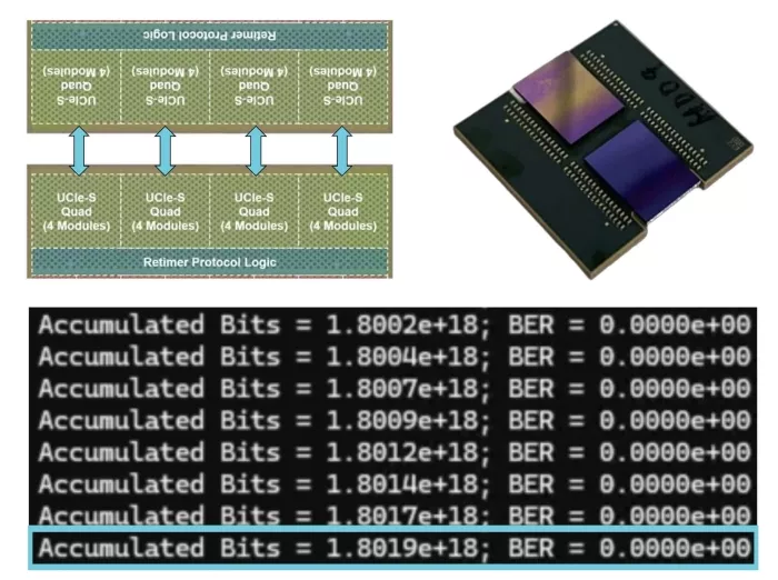
Figure 1. A dual-die package for UCIe testing and a five-day UCIe link test that resulted in the chiplets being error-free across all UCIe modules.
Optical Link Testing
EVT Link Margin Validation: In this test, a TeraPHY validation board and SuperNova board with module links were set up for cross-port optical loopback. The test found that optical links had 5+dB of margin across hundreds of links, even with SuperNova power per wavelength lowered to 2.5dBm
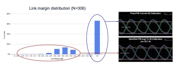
Figure 2. An EVT link margin validation test with the majority of optical links having 5+dB of margin.
Long-Term Link Stability: This test applied 5dB of attenuation to force bit errors on links and check BER over time. It provides a baseline for longer-running system tests. All links maintained stable BER over six hours, and some remained error-free for the entire time.
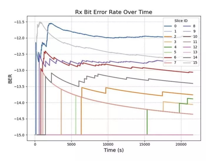
Figure 3. A long-term link stability test that results in all links maintaining stable BER for over six hours.
Thermal Cycling Link Test: This test evaluates how the TeraPHY chiplet reacts to changing temperatures. It starts at the baseline established in the previous test and then applies the temperature profile of liquid-cooled XPUs. The temperature was cycled up and down in the 30-80oC temperature range, representing the liquid-cooled XPU mission mode. It showed no BER dependence on temperature, and the majority of links were error-free for the duration. The chiplets’ thermal tuning subsystem successfully tracked all changes in temperature.
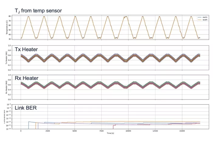
Figure 4. A thermal cycling link test resulted in no BER dependence on the temperature and the BER of all the links comfortably under the BER spec of 1e-12.
Application Testing
Co-packaged 500W ASIC Link Thermal Transients: This test measures how much of a temperature transient the link will be subjected to in typical working conditions. It simulates an ASIC or XPU increasing its power dissipation from 0 to 500W and observes the temperature change in the optical engine (which is about three millimeters away). In reality, the optical engines will be up to 25mm away from the XPU with the UCIe-S interface.
This produced a thermal transient with a brief rate peak of about 100 degrees C/s over a few degrees, after about 100 ms. The XPU itself maxed out at a 400 degrees C/s rate. This is the point where the thermal tracking loop is the most challenged.
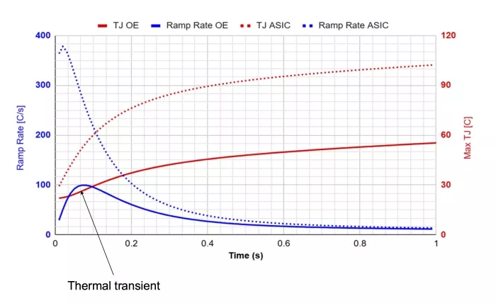
Figure 5. A link thermal transient test resulted in a brief thermal transient of about ~100oC/s.
Links up to 800 Degrees C/s (Emulated Hardware Test): This hardware test checks that the link remains stable over the high temperature transient observed in the previous test. It uses a tunable light source at variable sweeping rates from 10 to 50 nanometers (laser limit) to create the required ring resonance frequency movement equivalent to temperature ramps from 160 C/s to 800 C/s (eight times the maximum gradient seen in the previous test).
We found the subsystem is robust to extremely high sweep rates, far beyond what it would experience in a normal liquid-cooled system. There were essentially no bit errors for the duration of the ramp test; the tuning subsystem had to drive the ring resonator to keep track of the fast-moving laser, which is equivalent to compensating the ring resonance shift due to external temperature ramp, and Rx eye height as well as BER remained stable.
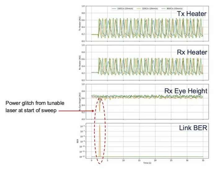
Figure 6. A co-packaged 500 W ASIC link thermal transient application study in which the tuning sub-system is tracking the emulated temperature (wavelength) changes and showing no bit errors for the duration of the ramp test.
UCIe over Optics End-to-End Link Test: As a final test, we use this dual-die package to create an end-to-end link from one die to another. In Package 0, one die (labeled UCIe Die 0) generates the data and sends it over the UCIe interface to the other die in the package (labeled TeraPHY Optical UCIe Retimer 0), which converts the electrical data to optical and sends it to Package 1, where the converse process happens—the TeraPHY Optical UCIe Retimer 1 chiplet converts optical data to electrical and sends it to UCIe Die 1 via UCIe interface, and UCIe Die 1 checks the data. Simultaneously, data gets generated and sent in the opposite direction. This tests the full link in both directions—two UCIe links with an optical link in between.
Full-duplex error-free BER was observed at every test point over more than 10 hours. The end-to-end latency from the leftmost data generator to the rightmost data generator was less than 25ns.

Figure 7. A block diagram that illustrates how data is transmitted and received across two packages.
In conclusion, following this battery of tests, we have completed the EVT validation of our latest TeraPHY optical engine. Onward to wrapping-up DVT!
The Connectivity Problem with Large-Scale AI Systems
Now let’s step back and review the bigger picture of where optical engines fit into solving the “beyond the rack” scale-up fabric connectivity challenge.
In March 2025, NVIDIA announced an “AI supercomputer” that it claims can scale to “tens of thousands” of GPUs. Building large-scale AI systems like this is fundamentally a connectivity problem. Connecting a rack’s worth of GPUs together requires about a meter of cable. That is the best copper can do at required data rates (200+ Gbps). A multi-rack setup takes 15 meters. An entire cluster needs about 100 meters. To turn anything beyond a single rack into an inference machine, you need optical I/O.
The bandwidth and latency needs of these systems make it impossible to run multi-rack or cluster-sized systems with electrical interconnects. Power is an even bigger issue. At GTC 2025, NVIDIA estimated a single rack would consume nearly 600 kW of power using electrical I/O. This trend is clearly not sustainable.
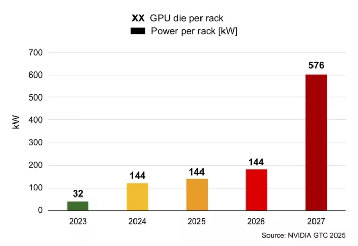
Figure 8. The power challenge of future AI systems: with each rack containing 576 GPUs and using electrical I/O, NVIDIA estimated that nearly 600 kW of power would be consumed.
Optical Engines Enable Scalable, Flexible, and Composable AI Infrastructure
This is where optical engines—particularly Ayar Labs’ TeraPHY UCIe optical chiplet—excel. It enables cluster-level GPU-to-GPU and GPU-to-switch connections to support the data movement and computing demands of large-scale AI models.
Optical engines offer increased reach, reduced power consumption, higher bandwidth density, lower latency, and higher radix than electrical interconnects. These factors become data movement bottlenecks when building inference clusters larger than a single rack of GPUs using electrical interconnects. The TeraPHY optical engine removes these bottlenecks.
This translates to significantly better interactivity per user and profitability (performance/TCO) for AI applications running on these scaled-up systems. As you can see here, the improvement from the previous generation of AI hardware using copper interconnects (red) to the next generation (purple) is dramatically smaller than the improvement gained by moving to an optical scale-up fabric, and eventually optically connected memory.
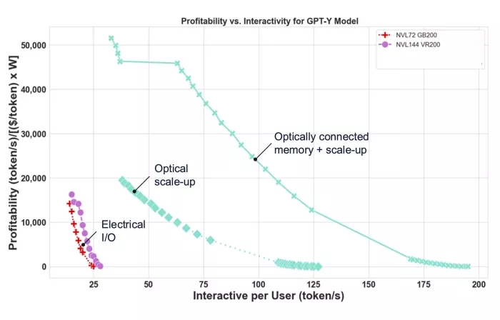
Figure 9. Profitability versus interactivity per user for a GPT-Y model.
Conclusion
As we continue marching down this path, quality and reliability tests are incredibly important for assessing the viability, stability, and robustness of our solution. This validation and a strong wafer sort process (another area where we have done pioneering work) are key to successfully manufacturing at scale.
UCIe optical I/O retimer chiplets have the potential to make AI optical scale-up possible—and these results show we’re well on our way. To learn more about how optical I/O can boost AI scale-up with higher bandwidth, increased power efficiency, and lower latency for enhanced AI performance, visit our AI scale-up solution page.
Related Chiplet
- High-Density Electronic-Photonic Chiplet
- DPIQ Tx PICs
- IMDD Tx PICs
- Near-Packaged Optics (NPO) Chiplet Solution
- High Performance Droplet
Related Blogs
- UMI: Extending Chiplet Interconnect Standards To Deal With The Memory Wall
- Accelerating the AI Economy through Heterogeneous Integration
- Advanced Packaging Evolution: Chiplet and Silicon Photonics-CPO
- AI and Semiconductor in Reciprocity
Latest Blogs
- Chiplets 101: An Arteris Guide to Multi-Die Architecture
- 2.5D + 3D = “3.5D”!
- Addressing AI and Advanced Packaging Challenges with Synopsys 3DIO PHY
- Ultra-high repeatability and ultra-low insertion loss wafer and die-level visible-range E-PIC device characterization using an MPI Corp. probe system, enabled by process optimization from Quantum Transistors
- The Changing ASICs Landscape: the Shift Toward Chip Disaggregation
