3D-ICs in the Automotive Market: Breaking Barriers with AI-Driven EDA Tools

The automotive industry is experiencing a significant transformation as it adopts innovations like autonomous driving technologies and ultra-connected ecosystems. At the core of this change is a rising demand for compact, high-performance semiconductor solutions that can handle the increasing complexity of modern vehicle architecture. One promising development is three-dimensional integrated circuits (3D-ICs), an innovative semiconductor design approach that has the potential to reshape the automotive market.
By vertically stacking multiple chips, 3D-ICs provide exceptional performance, bandwidth, and energy efficiency while overcoming the critical space and thermal limitations of vehicle systems. However, despite their potential, the design and implementation of 3D-ICs come with significant challenges. This is where AI-driven electronic design automation (EDA) tools play a crucial role, enabling engineers to explore new frontiers in 3D-IC innovation. Together, these technologies are creating new opportunities for automotive applications, ranging from advanced driver-assistance systems (ADAS) to infotainment platforms, ultimately paving the way for the vehicles of the future.
Pioneering Semiconductor Advancements
The role of semiconductors in automotive innovation cannot be overstated. Silicon technologies such as silicon carbide (SiC) and gallium nitride (GaN) have transformed power electronics, delivering high efficiency at reduced energy losses. These advancements are critical for electric vehicles (EVs) and hybrid systems, where performance and energy optimization are paramount. However, as the industry pushes toward advanced nodes (e.g., 3nm or 5nm processes), significant challenges emerge:
- Rising Costs: Advanced nodes demand higher fabrication costs, leading to increased cost per transistor. This trend disrupts the traditional cost-efficiency promised by Moore's Law.
- Yield Limitations: Larger chip designs result in lower yield rates, making larger SoCs increasingly impractical.
- Complexity of Analog and RF Circuits: Analog circuits and radio-frequency I/Os are often less compatible with advanced node technologies due to inherent design complications.
- Memory Bandwidth Bottlenecks: The need for high-speed memory access has spurred innovations in high-bandwidth memory (HBM) integration and chip stacking, bringing memory closer to the processing core for increased performance.
How AI-Driven EDA Tools Are Changing the Game
To address these challenges, the industry is adopting disaggregated solutions, breaking down large SoC designs into smaller chiplets. These chiplets are interconnected through robust interfaces like UCIe, forming modular systems. This approach ensures better cost management, improved performance, and design flexibility. And more importantly, AI-powered EDA tools step in—not as an evolution, but a revolution. These next-gen platforms bring intelligence and automation into the complex process of designing 3D-ICs.
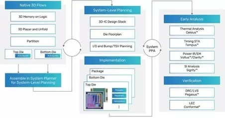
AI-driven EDA tools are redefining the landscape of semiconductor design, particularly in the era of 3D-ICs and modular chiplets. These innovative platforms are not just advancing, but fundamentally transforming the design process with their ability to integrate intelligence and automation into traditionally complex workflows. By leveraging advanced and intelligent features, EDA tools can enable a design environment that successfully navigates the challenges of disaggregated systems. Such an environment must seamlessly connect chip and package domains while ensuring the modular assembly of multiple chiplets for bottom-up integration and providing a top-down system perspective for effective partitioning. The inclusion of features like early system-level feedback on factors such as thermal behavior and power dissipation ensures that design intent is maintained throughout, driving convergence across the chip-package ecosystem. This holistic approach is empowering designers to achieve unprecedented levels of performance, flexibility, and efficiency in multi-die systems.
The Role of AI-Driven Integrated Design Platforms
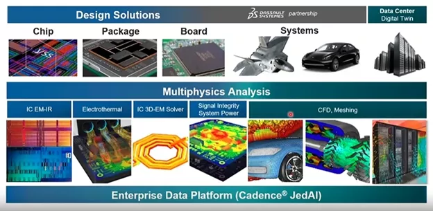
Traditional disjointed workflows, with separate tools for IC, PCB, and package design, have amplified inefficiencies such as data inconsistencies, error-prone processes, and lengthened design cycles. To address these limitations, Cadence's AI-driven Integrated 3D-IC Platform offers a unified and highly collaborative environment that integrates all design domains into a coherent workflow. This enables teams to optimize performance, power, and thermal interactions early in the process, mitigating costly redesigns and improving time to market.
Tackling Complexity with Cross-Domain Collaboration
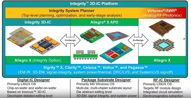
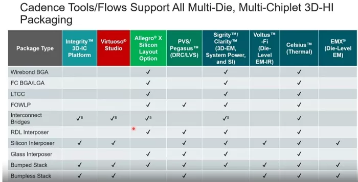
Modern automotive and high-performance systems depend on seamless coordination between diverse components like processors, memory, interconnects, and power systems. With the integrated 3D-IC platform, Cadence breaks down design silos, offering tools like the Virtuoso Studio, Innovus+ Synthesis and Implementation System, Allegro X Design Platform, and the Sigrity X Platform for specialized tasks—all synchronized under a centralized database. This level of integration ensures that co-design processes are cooperative rather than isolated, allowing engineers to visualize and analyze system-wide interactions effectively.
For example, the platform enables package and PCB engineers to work directly alongside IC designers, identifying signal integrity issues or thermal hotspots across chip-stack layers early in the workflow. This consistency ensures that simulation and implementation workflows remain closely aligned, reducing design risks and eliminating redundant iterations.
Shift-Left Methodologies for Enhanced Efficiency
Cadence's proactive approach prioritizes the "shift-left" methodology, which emphasizes front-loading critical analyses like thermal, signal integrity, and power performance. By integrating these checks earlier in the design cycle, engineers achieve both efficiency and precision. This methodology enables immediate identification of issues such as voltage droop or electromagnetic interference in high-density automotive radar systems, significantly reducing downstream bottlenecks.
Complementing this is the Cadence Assembly Design Kit (ADK), which provides standardized templates and compliance rules tailored to specific process technologies. These kits empower engineers to start with robust design foundations, minimizing repetitive tasks and maximizing engineering resources toward project innovation.
Intelligent Automation and Data-Driven Optimization
Embedded within the Integrated 3D-IC Platform is the Cadence JedAI Solution, an AI-powered analytics system designed to further streamline and enhance complex workflows. By leveraging machine learning-based predictive analytics, Cadence JedAI automates key processes such as design rule checks and timing analysis, saving valuable engineering time. Furthermore, it identifies potential bottlenecks or critical paths across design iterations by analyzing historical trends, enabling designers to make informed decisions based on data-driven insights.
Cadence JedAI's capabilities are particularly impactful for evolving systems such as 5G base stations and AI accelerators, where performance optimization and tight design tolerances are critical. By harnessing intelligent automation, Cadence's platform ensures that these industry-specific designs are not only feasible but are also completed efficiently and accurately.
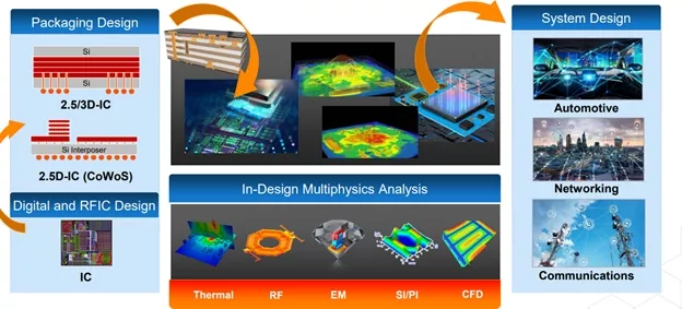
Tailored Solutions for Advanced Packaging
Advanced packaging is a key enabler of 3D-IC architectures, and Cadence supports a range of packaging technologies, including silicon interposers, fan-out wafer-level packaging, and even bumpless stacking methods. The platform allows for innovative workflows such as silicon-to-silicon routing, trench capacitor integration, and cross-die power delivery optimization. For RF systems in particular, its Virtuoso Studio-integrated workflow addresses parasitic-induced performance degradation by simulating accurate results in conjunction with PCB and package designs.
By offering these tailored solutions, Cadence redefines how industries can design heterogeneous, high-performance systems effectively. By eliminating siloed engineering processes and providing a suite of cutting-edge, AI-driven tools, the Cadence Integrated 3D-IC Platform ensures that complex challenges in the automotive, telecommunications, and AI markets are met with confidence and precision.
The Road Ahead: AI + 3D-ICs = The Future of Automotive Chips
The convergence of 3D-IC packaging and AI-powered design is set to redefine automotive electronics. As vehicles become smarter, safer, and more connected, the underlying silicon must evolve—and 3D-ICs offer the perfect foundation.
But without intelligent EDA solutions, the design complexity could stall innovation. The good news? AI is rising to the challenge, providing automotive chipmakers the tools they need to accelerate development, cut costs, and ensure reliability in mission-critical applications.
Learn more about how EDA tools and methodologies have evolved to address the challenges associated with advanced chiplet and multi-die package architectures in this CadenceTECHTALK by AE Group Director, Dr. Martin Biehl.
Related Chiplet
- DPIQ Tx PICs
- IMDD Tx PICs
- Near-Packaged Optics (NPO) Chiplet Solution
- High Performance Droplet
- Interconnect Chiplet
Related Blogs
- Breaking Through Bottlenecks: Executives from AMD, Ayar Labs, Cerebras, and Microsoft, Discuss the Future of AI Infrastructure with Optical I/O
- The Need for Chiplets, and UCIe in Automotive
- Chiplet Integration in the Automotive Realm
- Driving the Development and Deployment of Chiplets in the Automotive Industry
Latest Blogs
- Advancing High‑Performance Silicon Photonics and Silicon Germanium (SiGe) for the Next Era of Optical Connectivity
- Accelerating Chiplet Innovation with a New Partner Ecosystem
- Accelerating Multi-Die Innovation: How Synopsys and Samsung are Shaping Chip Design
- Six critical trends reshaping 3D IC design in 2026 and beyond
- AI Energy Gap and Chiplets: Why Data Movement Matters