MFIT : Multi-FIdelity Thermal Modeling for 2.5D and 3D Multi-Chiplet Architectures
By Lukas Pfromm∗, Alish Kanani∗, Harsh Sharma, Parth Solanki, Eric Tervo, Jaehyun Park, Janardhan Rao Doppa, Partha Pratim Pande, Umit Y. Ogras
∗ Equal contribution
L. Pfromm, A. Kanani, E. Tervo and U. Y. Ogras are with the Department of Electrical and Computer Engineering, University of Wisconsin–Madison, WI, USA.
H. Sharma, J. R. Doppa and P. P. Pande are with the School of Electrical Engineering and Computer Science, Washington State University, WA, USA.
P. Solanki and E. Tervo are with the Department of Mechanical Engineering, University of Wisconsin-Madison, WI, USA.
J. Park is with Department of Electrical, Electronic and Computer Engineering, University of Ulsan, Republic of Korea.
Abstract
Rapidly evolving artificial intelligence and machine learning applications require ever-increasing computational capabilities, while monolithic 2D design technologies approach their limits. Heterogeneous integration of smaller chiplets using a 2.5D silicon interposer and 3D packaging has emerged as a promising paradigm to address this limit and meet performance demands. These approaches offer a significant cost reduction and higher manufacturing yield than monolithic 2D integrated circuits. However, the compact arrangement and high compute density exacerbate the thermal management challenges, potentially compromising performance. Addressing these thermal modeling challenges is critical, especially as system sizes grow and different design stages require varying levels of accuracy and speed. Since no single thermal modeling technique meets all these needs, this paper introduces MFIT, a range of multi-fidelity thermal models that effectively balance accuracy and speed. These multi-fidelity models can enable efficient design space exploration and runtime thermal management. Our extensive testing on systems with 16, 36, and 64 2.5D integrated chiplets and 16×3 3D integrated chiplets demonstrates that these models can reduce execution times from days to mere seconds and milliseconds with negligible loss in accuracy.
Introduction
Massive data from different modalities, including text, images, video, and speech, are continuously produced by various sensors. At the same time, increasingly complex artificial intelligence (AI) and machine learning (ML) algorithms process this data to enable new applications that were previously impractical. This trend dictates the design of large-scale chips with high memory and compute capabilities, offering a high degree of parallelism [1, 2]. Traditional 2D chip design and packaging technologies cannot sustain this need due to the low yield of large monolithic planar chips and the corresponding increase in fabrication cost [3]. Therefore, new design approaches are required to meet the increasing demand for computing power and memory capacity.
2.5D and 3D chiplet-based architectures have emerged as promising alternatives to traditional monolithic 2D chips due to their lower fabrication costs [4, 5, 6]. Compared to conventional monolithic systems, chiplet-based systems integrate multiple small pre-fabricated chips (chiplets) on a silicon interposer, which facilitates data exchange, as illustrated in Figure 1(a). 3D packaged systems expand on this approach by stacking multiple chiplets vertically and connecting them with vertical vias, creating a more compact system as illustrated in Figure 1(b). The smaller size of these chiplets enables a higher yield and lower overall manufacturing cost than traditional monolithic dies [7]. Additionally, this modular approach facilitates scaling the system sizes and enables heterogeneous integration of different chiplet types, e.g., memory, processing, and processing-in-memory chiplets. Hence, emerging 2.5D and 3D architectures enable a new cost-effective avenue for compact scale-out implementations of various emerging compute- and data-intensive applications, including AI/ML. Indeed, these advantages have led to industrial adoption by companies including Intel, AMD, and NVIDIA.
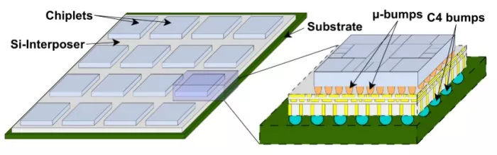
(a) A 16 - 2.5D integrated chiplet based system. The magnified view on the right shows a detailed structure of a single chiplet.
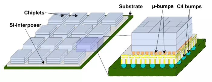
(b) A 16×3 - 3D integrated chiplet based system. The magnified view on the right shows a detailed structure of three chiplets stack.
Figure 1: 2.5D and 3D integrated chiplet systems considered in this work, showing the chiplets, interposer, and a portion of the substrate.
Thermal bottlenecks have long been a significant barrier to increasing the performance of computing systems. 2.5D and 3D integrated systems exacerbate this barrier due to their dense integration and unique physical structure [13]. In contrast to a monolithic chip, where heat is spread directly across the die, a 2.5D chiplet-based system conducts heat between different chiplets through the interposer and heat spreader. Likewise, heat also flows vertically between adjacent stacked chiplets in a 3D chiplet-based system.
These factors introduce unique challenges for effective thermal management in these systems. Traditional design flows and physical floor planning focus on reducing wire lengths to meet timing constraints and minimizing area to reduce fabrication costs. However, these objectives could also lead to thermal crosstalk, thermal hotspots, and compromise performance. Chiplet-based systems introduce additional design parameters such as inter-chiplet link length, spacing, chiplet placement, sizing, inter-layer communication, and design partitioning. Tuning traditional and chiplet-based design parameters while maintaining thermal stability is critical to ensure a thermally-efficient design.
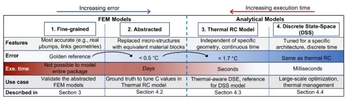
Figure 2: Summary of the multi-fidelity thermal models. (1) Fine-grained FEM models capture precise geometry but are too complex to simulate the entire chiplet-based system. (2) Abstracted FEM models are derived from the fine-grained model to simulate large-scale systems with negligible impact on accuracy. (3) Since abstract FEM models are still too slow for DSE, they are used to tune thermal RC circuit models. (4) Further abstraction reduces the execution time to milliseconds using DSS models created for specific system configurations, enabling runtime thermal management.
The semiconductor chip design cycle spans multiple phases: system specification, architecture exploration, logic design, physical design and validation, fabrication, and post-silicon optimization/validation. Each phase has a unique set of design constraints and requirements. For example, lacking a test chip during the pre-silicon phases requires simulation and analytical models. Finite Element Method (FEM) simulations offer the most accurate approach for pre-silicon thermal analysis [14]. They can serve as a reference and enable heat flow studies to guide the design process. However, they are too slow for practical architecture and design space exploration (DSE). Modeling the package as a thermal RC (resistive-capacitive) network can significantly accelerate simulations with acceptable accuracy loss [15, 16]. Since each node in the thermal circuit corresponds to a specific location in the package, thermal RC models solve discretized versions of the FEM models in space. Hence, they enable thermally-aware DSE and optimization with a finite number of discrete hotspot nodes. However, the thermal resistance/capacitance values and the circuit topology must accurately reflect the chip geometry and material properties for reliable results. Since the thermal RC models solve continuous-time ordinary differential equations (ODEs), they have execution times in the order of seconds to minutes. Therefore, they cannot be used for runtime optimization tasks such as dynamic thermal and power management (DTPM). One can discretize them in the time domain with a given sampling period [17, 18]. The resulting discrete state-space (DSS) models significantly reduce runtime at the cost of further abstracting the model from the physical package. Consequently, they are applicable only to the specific configurations for which they are developed.
There is a strong need for tools to accurately analyze the thermal behavior of 2.5D and 3D integrated systems and guide their design process. However, no single modeling technique can alone address the needs of all design phases. To address this much needed gap, this paper proposes MFIT, a multi-fidelity thermal modeling framework that synergistically exploits the strengths of each class of models (FEM, thermal RC, and DSS). We use this framework to produce a set of thermal models that can guide the entire design cycle, unlike a point solution that can serve a specific portion of the design process. The elements of this set not only cover complementary parts of the design cycle but support each other and produce consistent results. We first develop a fine-grained FEM model of the target package as a reference. Since it is slow and computationally expensive, we next judiciously design an abstracted version of this fine-grained FEM model to simulate an entire package in days while maintaining accuracy. To enable fast DSE, MFIT also incorporates thermal RC circuit models verified against the reference FEM models. Our thermal RC models run in the order of seconds while leading to less than 1.7∘C error, as summarized in Figure 2. Hence, they can be used for pre-silicon architectural optimization, such as mapping the workloads to chiplets, network-on-interposer design, and chiplet placement for 2.5D and 3D stacked systems. Finally, MFIT derives one more class of models by discretizing the thermal RC models, enabling runtime thermal management and large-scale DSE in the order of milliseconds. However, they work only for a specific sampling period and configuration. Hence, the parameters must be regenerated from the RC model if the target configuration changes. In summary, we obtain a set of multi-fidelity thermal models that guide and complement each other to cover all design phases.
The key contributions of this work are as follows:
- A novel thermal modeling approach that systematically abstracts fine-grained FEM models to produce abstract FEM, thermal RC, and DSS models to achieve varying speed and accuracy trade-offs,
- A family of open-source multi-fidelity thermal models that span a wide accuracy (reference to 1.7∘C) and speed (days to milliseconds) range,
- Extensive evaluations with 16, 36, and 64 - 2.5D and 16×3 - 3D integrated chiplets systems running AI/ML workloads to demonstrate the accuracy and speed-up benefits of our multi-fidelity thermal models,
- Open-sourced code for thermal RC and DSS models at github.com/AlishKanani/MFIT. Additionally, we plan to make our FEM models publicly accessible in the near future.
The remainder of the paper is organized as follows. Section II and Section III discuss related work and background on FEM. Section IV presents the proposed multi-fidelity thermal modeling framework. Finally, Section V presents the experimental evaluation, and Section VI concludes the paper.
To read the full article, click here
Related Chiplet
- DPIQ Tx PICs
- IMDD Tx PICs
- Near-Packaged Optics (NPO) Chiplet Solution
- High Performance Droplet
- Interconnect Chiplet
Related Technical Papers
- 3D-ICE 4.0: Accurate and efficient thermal modeling for 2.5D/3D heterogeneous chiplet systems
- 3D Stacked HBM and Compute Accelerators for LLM: Optimizing Thermal Management and Power Delivery Efficiency
- Lifecycle Cost-Effectiveness Modeling for Redundancy-Enhanced Multi-Chiplet Architectures
- CHICO-Agent: An LLM Agent for the Cross-layer Optimization of 2.5D and 3D Chiplet-based Systems
Latest Technical Papers
- Making Locality-aware GEMM Compatible with Page-Granularity Placement on Chiplet GPUs
- Advanced semiconductor packaging design via artificial intelligence and machine learning: A review
- DTCO of NOR-Type IGZO FeFETs for 3D Heterogeneous AI Memories: A Read-Centric Perspective
- Modeling, Optimizing and Exploring Multi-Die FPGA Routing Architectures
- A 32 Gb/s 0.41 pJ/bit Single-Ended Transmitter with TX-Based-Only Adaptive Crosstalk Cancellation for Ultra-Short-Reach Wireline Applications