Deploying Chiplets into Mass Markets
By YorChip
Abstract
Chiplets are being universally used in highest performance SOC, ASICs and ASSP devices by large integrated Semiconductor companies to reduce costs and increase yields. However, we have not seen the expected rapid deployment of standardized Chiplet building blocks that designers can simply buy and deploy cost effectively, much faster than developing a traditional SOC.In this paper we review key roadblocks to rapid adoption and provide five detailed suggestions to overcome barriers.
I. INTRODUCTION
Let’s start with a quick limited introduction to chiplets. A very good intro is the ODSA Business Group Whitepaper [1].
In this paper they show the substantial cost reduction by disaggregating a 25.8 x 25.8mm single die into 2 chiplets. See Figure 1 below.
Their numbers show a 40% overall cost reduction. Splitting into 4 smaller chiplets of 14.5mm x 14.5mm2 will show an even more dramatic cost reduction.
The overall cost reductions are compelling and it’s fair to say that almost every large HPC semiconductor device being planned today is planning on using chiplet methodology as the ROI is very clear.
Coupled with almost universal use of Chiplets are advances in advanced packaging supporting 3D stacking, improved technology for smaller bump maps, better substrate advances which support the rapid market adoption.
Die2Die links have evolved rapidly to push beyond 16G per link to 32G per link starting to become prevalent. The accepted view is multi-Terabit links are the future and technology vendors are rapidly supporting it.
New standard interfaces to ease interoperability such as UCIe have been introduced with much fanfare and rapidly supported by foundries, OSATs, and IP developers.
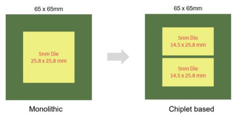
Fig. 1. From ODSA business paper – showing disaggregation
II. CHIPLET DOMINATION
Forecasting technology markets is not easy, but the case for Chiplets seems compelling based on HPC traction. see figure 2 below for representative forecasts.
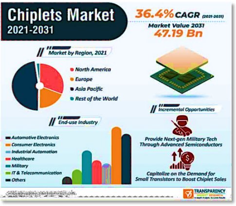
Fig. 2. Market Forecast
An example forecast is above [2]showing Chiplets moving on into a wide range of applications from Automotive to Consumer to Military on a world-wide basis. And a rapid projected compound growth rate of 36%+ which is a reasonable projection considering Chiplet domination in HPC.
The one key assumption by most forecasters is that there will be simple follow through of this technology to lower performance markets as costs naturally decrease and technology matures.
III. ROI REDUX
If one repeats the cost reduction exercise with Chiplets that are manufactured in older technology Nodes and smaller chiplets are used such as 5x5mm the cost reduction turns into an addition. The major problem is cost of advanced packaging, mask costs of multiple designs versus a single SOC are difficult if not impossible to overcome.
Perhaps why Open Market Chiplets do not yet even exist today, and mass market adoption may never occur.
A promising memory technology HBM has only seen limited traction due to costs of advanced packaging outside of HPC market – this may be future of Chiplets in Mass Markets.
IV. INNOVATION
In our view the multi-Terabit technology being development for HPC will not easily scale down to Mass Market. And a more methodical approach is needed to advance Chiplets by innovating on total cost, security, and time to market. These innovations we believe will enable meaningful ROI for Chiplets to win in Mass Markets adoption.
A. Size Matters – ONE SIZE for ALL does not work
At YorChip we are developing a multi-Gigabit PHY that scales easily from 4 lanes to 32 lanes. Area is 0.25 mm2 vs 1.6mm2 for UCIe and BOW for 4 lane version see figure 3 below.
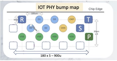
Fig. 3. YorChip’s cost optimized PHY
At YorChip we plan to work with OCP and UCIe to move the industry to consider flexible PHY solutions to enable wider adoption.
B. IP & Older Nodes Matter
PHY’s must support older Nodes as Mixed Signal IP is difficult to scale and redesign. By easing a path to leverage existing IP and deploying advanced PHY’s we can increase the quality and quantity IP availability for Chiplets market.
C. Packaging Cost Reduction
As an industry we must consider and develop alternatives to interposers and expensive substrates. Simply put if the die cost is a fraction of the packaging cost, we are not going to have a viable ROI.
At YorChip we are exploring novel packaging options for Chiplets – and the industry needs to focus on this issue.
Chip Scale Packaging is an interesting option that is very low-cost results in very small area utilization. It enables great electrical characteristics with proven reliability and quality.
It is a great option to solve the risk issues of KGD, and costs of substrate design and manufacturing in modest to high volumes for mass adoption.
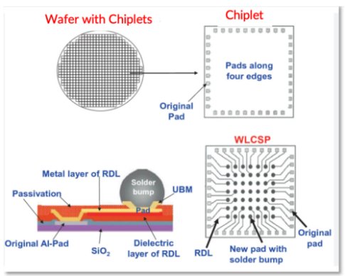
YorChip is enabling a patented option of higher ESD PHY solution (selectable by RDL) which enables Chiplets to be deployed in Chip Scale Packaging.
Customers can build micro (uASSP) products and end customers will save time and money developing their products with excellent ROI.
D. Redundancy
Both UCIe and BOW have redundancy options for advanced packaging but none for standard packaging.
At YorChip even our smallest PHY the 4 lane IOT includes redundancy. The R bump at top left is the spare bump for our redundancy support. When one Chiplet link failure can force a scrap of the whole module - hence a critical area for Chiplet adoption. This is especially important for an open market where customers will purchase disparate Chiplets from multiple vendors and supply chain is uncertain.
E. SUPPLY Chain and SECURITY
There is a lot of concern in the industry about securing the supply chain and securing semiconductors devices.
This is a golden opportunity for Chiplets to offer a KGD solution but unfortunately there is no agreement on a standard.
Currently the UCIe and BOW standards fail to support security for data or supply chain.
At YorChip we build security into our PHY as well as manufacturing data which can be easily read during wafer probe – See Bump P at bottom right of our PHY. This is a patented feature, but we encourage the industry to develop strategies and technology standards to enable security and supply chain support.
Related Chiplet
- DPIQ Tx PICs
- IMDD Tx PICs
- Near-Packaged Optics (NPO) Chiplet Solution
- High Performance Droplet
- Interconnect Chiplet
Related Technical Papers
- Extending network-on-chip (NoC) technology to chiplets
- Heterogeneous Integration - Chiplets
- Challenges and Opportunities to Enable Large-Scale Computing via Heterogeneous Chiplets
- Chiplets for Automotive – Are We There Yet?
Latest Technical Papers
- LEXI: Lossless Exponent Coding for Efficient Inter-Chiplet Communication in Hybrid LLMs
- Link Quality Aware Pathfinding for Chiplet Interconnects
- Effects of Poor Workload Partitioning on System Performance for Chiplet-Based Systems
- Mozart: Modularized and Efficient MoE Training on 3.5D Wafer-Scale Chiplet Architectures
- Network Design for Wafer-Scale Systems with Wafer-on-Wafer Hybrid Bonding