Business Analysis of Chiplet-Based Systems and Technology
Marek Hempel, Analog Devices
Anu Ramamurthy, Microchip
Kash Johal, YorChip
Trent Uehling, NXP
James Wong, Palo Alto Electron, Inc.
Irina Sellhusen, Process Dynamics LLC.
Rajesh Pendurkar, University of California Santa Cruz
Boon Chong Ang, Intel
Allan Cantle, Nallasway Inc.
Bapi Vinnakota, Open Compute Project
Abstract
Chiplet-based design is reshaping the way we build semiconductor systems with the promise to develop products cheaper, at lower unit cost and with faster time to market. These benefits and reports of success stories from big industry players are well documented in literature. However, successfully adopting a chiplet-based design needs to be a carefully made decision depending on a variety of interconnected factors that are often only cursively discussed. This disconnect was evaluated by a talk series of 9 companies sharing their business challenges to implement chiplet systems, in the Open Domain Specific Architecture (ODSA) Sub-Group of the Open Compute Project. As a response, the business work stream of the ODSA compiled this whitepaper which offers insight into what technology choices exist and how to model the cost and return of chiplet-based versus monolithic design. We summarize chiplet architecture choices, explain the tight interplay between die-to-die interfaces and packaging technology, highlight the importance of probe and test and offer a holistic view of a chiplet cost structure model. Additionally, we examine the requirements for an open chiplet market place and point out the critical role of chiplet design standardization. Taking these insights into account will enable system architects and product managers to make more informed decisions about when to use chiplet-based product design.
Executive Summary
As the semiconductor industry faces challenges in maintaining Moore's Law due to shrinking transistors becoming economically challenging, it is turning towards smaller, modular "chiplets." These chiplets, designed for specific functions, can be interconnected to build systems, offering advantages like reduced defects and manufacturing costs. However, the broader adoption of chiplets is hindered by challenges in standardization, particularly in facilitating the combination of chiplets from different manufacturers. Balancing cost and performance remains a significant challenge, influenced by chiplet architecture, die-to-die interfaces, packaging, and testing.
The architecture of chiplet-based systems plays a crucial role in influencing system area, cost, power, and performance. Two integration categories, heterogeneous and homogeneous, offer different advantages. Heterogeneous systems leverage diverse process nodes, providing benefits in power, performance, and area through IP reuse and faster time to market. On the other hand, homogeneous systems reduce die size and enhance yield by employing smaller die in the same process technology. Standardized chiplet interfaces are essential for achieving reusability and enabling a mix-and-match capability. Various die-to-die interfaces, including open standards like Bunch of Wires (BoW) and Universal Chiplet Interface Express, play a role in interoperability, with considerations for bandwidth, power consumption, and cost influencing the choice of a chiplet interface.
Testing semiconductor dies is crucial for enhancing product reliability and reducing costs. Design for Testability (DFT) techniques, such as At-speed Scan, ATPG, BIST, and boundary scan, are employed at the chip/chiplet level. The target test cost is set not to exceed 20% of the product die cost. Chiplet systems offer cost-effectiveness for large dies on cutting-edge process nodes, benefiting from improved yield at smaller die sizes. The adoption of chiplets in leading-edge devices is driven by economic and system scalability benefits. The emergence of open standards like BOW and UCIe promises an Open Chiplet Market, allowing for off-the-shelf chiplets to be purchased for custom devices or faster system development. However, interoperability and security are crucial for the Open Chiplet Market to thrive, and challenges in the supply chain, packaging, and device qualification pose barriers to adoption.
The Chiplet Design Exchange (CDX) workstream advocates for standardized chiplet models, an open standard data format, and detailed integration workflows for effective chiplet utilization and higher-quality designs. Proactive planning is crucial for businesses to optimize returns on chiplet-focused investments and commercialization plans.
1. Introduction
Chiplets are a design methodology to build systems out of modular die (chiplets) with standardized interfaces. This approach promises to bring semiconductor products to market faster, cheaper and with lower unit cost. Chiplets are estimated to be a $48B market in 2024 that will grow to $204B by 2032, according to Yole [1]. Today, chiplets are used predominantly by large, vertically integrated companies for high-performance, high-volume applications. However, in the future, they are seen as a way to enable customized high-mix low-volume systems through Lego-like integration of chiplets from different vendors into a single package.
Designing chiplet-based systems is not trivial. Determining whether this architecture is a good fit for a given application must be decided on a case-by-case basis and is often linked to a company's broader product strategy. It also requires tighter interaction across the semiconductor design cycle as design choices now strongly interact with downstream disciplines like packaging and test, as shown in Figure 1.
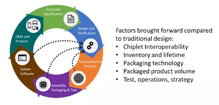
Figure 1: Semiconductor design cycle requiring strong interactions for chiplet-system design.
Many recent white papers and reviews introduce the key benefits and challenges of chiplets [2-7]. However, there is less literature guiding interested product groups on how to analyze the trade-offs between a monolithic or chiplet-based approach. This whitepaper attempts to shed light on the implications of using chiplets from a business perspective. Aside from the more obvious chiplet benefits like yield improvements, it seeks to elucidate the trade-offs of using chiplets in cost-constrained applications and for the sake of modularity. The whitepaper is a response to the ODSA chiplet business challenges talk series [8] from spring 2023, where nine participating companies shared their challenges of adopting chiplets.
The white paper starts by providing background information on the various aspects, from product architecture to packaging and testing that need to be considered. It then describes a chiplet cost structure and standardization efforts that will help teams interested in chiplet development adequately analyze and justify this design choice. Lastly, this whitepaper discusses some aspects of what will be needed for an open chiplet marketplace that goes beyond individual companies’ design chiplets for their own products.
2. Chiplet Architecture
The architecture of a chiplet-based system has a significant impact on the area, cost, power and performance of the system itself. Therefore, it must be thought through well at the start of the design cycle. The process of architecting also provides potential ideas for the various chiplets that compose the functional system. The selection of the various chiplets that make up the system affects decisions about the D2D (Die-to-Die) interface, the package, and hence the cost. In some cases, there are obvious boundaries like the CPU, memory, and IO. In other cases, a point of disaggregation has to be specifically defined to take advantage of smaller die or older process nodes while carefully considering trade-offs such as D2D interface, area impact, cost impact, chiplet node selection, and future chiplet re-use.
There are two broad categories for a chiplet system to come together. The first is a heterogeneous integration, which involves combining chiplets optimized in different process nodes. The second is a homogeneous integration, slicing of a larger SoC into pieces to reduce die size and improve the yield.
Heterogeneous Systems
Typically, heterogeneous systems are disaggregated by function (different nodes), see Figure 2. Each function can be optimized in a different process node/foundry etc. Most analog functions don't gain much Power/Performance or Area benefits from scaling at leading edge process nodes. They can remain in larger process nodes with a mature process that has high yields and low cost of silicon. The digital functions that require very high performance, smallest area and power will benefit greatly from moving to cutting edge process nodes. The trade-off in cost of reducing silicon die cost but increasing the assembly cost of integrating the die onto a common package often proves to result in an overall reduction in the cost of this heterogeneous system.
Heterogeneous chiplet systems also enable the concept of re-use of IP (Intellectual Property). The functional chiplets are relatively easy to integrate into new Systems with a similar D2D interface. Even more attractive is the fact that this IP is silicon-proven, this can enable a reduced test vector set during wafer sort and final package test, hence lowering test cycle time and test cost. The reuse concept also can be extended to the ability to assemble different variants of the product by mixing and matching.
This could dramatically improve the Time to Market (TTM) for multiple products. The benefits of reduced design cycle time and a faster time to market indicate that resources that would in the case of a monolithic SoC design be busy integrating the various functions together on Silicon are now free to work on a different/new design/skew or product. We can define this as opportunity cost.
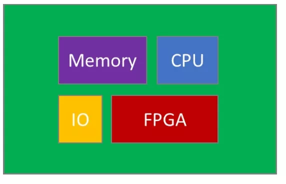
Figure 2. Example of a disaggregated system into functional blocks.
Homogeneous Systems
Tiled design typically takes advantage of smaller die in the same process technology, which is then connected via D2D interfaces. Each slice could be identical as in the case of Xilinx in Figure 3, where a large FPGA was sliced into 4 pieces and had about 10,000 D2D connections between each slice. They could also be disaggregated by function (e.g. Logic, IO) - Such systems could also be functional blocks in the same process technology again to take advantage of higher yielding smaller die, as exemplified by AMDs CPU product strategy [5].
This type of integration also lends itself to the re-use of IP to create multiple SKUs (Stock Keeping Units) and products as outlined in the section on Heterogeneous Integration.
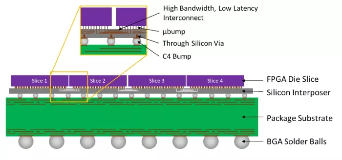
Figure 3: Cross-section of a Xilinx Virtex FPGA using homogeneously integrated chiplets [9].
3. Die-to-Die Interfaces
Standardized chiplet interfaces are crucial to make chiplets reusable and enabling Lego-like mix-and-match capability. A chiplet interface is organized into four layers: the physical layer, the link layer, the transport layer, and the protocol layer. Generally, all these layers of two individual chiplets need to be compatible to ensure interoperability. Another possibility is the use of an FPGA chiplet to act as a bridge between two different protocols or interfaces, as discussed further in Section 7. There are many die-to-die interfaces to choose from, both open and proprietary standards. The leading open interfaces in 2023 are Bunch of Wires (BoW) [10] and the Universal Chiplet Interface Express [11] which are designed for interoperability. Examples of proprietary D2D interface from different IP providers include Ultra-Link (Cadence) [12], DesignWare (Synopsys) [13], GLINK (GUC) [14], or Glasswing (Kandou) [15], many of which are based on extra-short, or ultra-short reach SerDes (XSR/USR) [16] defined by the Optical Internetworking Forum (OIF).
There are many parameters to compare to choose a chiplet interface. They include bandwidth range indicating the total data throughput in gigabits per second (Gbps), the beachfront describing the linear edge data density (Gbps/mm), the PHY footprint (mm2), the power consumption per bit (pJ/bit), the data transfer latency (ns), and the maximum allowable distance between chiplets (mm). Other related aspects are the required packaging technology and associated cost, the level of adoption, the maturity of the interface, and the availability of IP on different nodes for a given interface. The next four paragraphs summarize the different design choices around AIB, BoW, UCIe, and XSR/USR. A summary is provided below in Table 1. Additionally, an ODSA subgroup has created a comparison table of D2D PHYs [17] in 2020 including open-source and proprietary interfaces. A revision of this table is currently underway.
| Die-to-Die Interface | Ultra Short Reach SerDes (XSR/USR) | Bunch of Wires (BoW) | Advanced Interface Bus (AIB) | Universal Chiplet Interface (UCIe) |
| Adoption | Industry standard / in production | ~ 10 companies designing with BoW | ~ 10x3rd party chiplets, Intel’s chiplets | ~120 member companies |
| Package | laminates | standard, advanced, | advanced packaging | standard, advanced |
| Bump Pitch | 130-170 μm | 45-170 μm | 25 - 55 μm | 10-130 μm |
| Lane Rate | 112 G / 224 G | 2 - 32 Gbps | 2 - 6.4 Gbps | 4 - 32 Gbps |
| Latency | ~10 ns | < 2 ns | < 2 ns | < 2 ns |
| Reach | < 50 mm | < 25 mm | < 25 mm | < 10 mm |
| Bit Error Rate | <1E-15, <1E-6 w/ FFC | <1E-15 | n/a | <1E-15 to <1E-27 |
| Energy | 1-4 pJ/bit | 0.3-0.5 pJ/bit | 0.5-0.8 pJ/bit | 0.25-0.5 pJ/bit |
| Edge Density | < 3 Tbps/mm | < 4 Tbps/mm | < 1.6 Tbps/mm | < 10 Tbps/mm |
| Link Layer | Not Defined | BoW link layer, supporting AXI, CHI | AXI | Raw, Streaming, PCIe, CXL |
| Target Applications | Optical Networking | Disaggregation, e.g AI accelerators, automotive | Aerospace & defense ecosystem | Scale & split, system aggregation |
Table 1: D2D Interface comparison between AIB, BoW, UCIe, and XSR/USR.
The Advanced Interface Bus (AIB) is an open-source chiplet interface pioneered by Intel and used in its Stratix and Agilex FPGA, now part of the Chips Alliance (Linux Foundation). Several partner companies have developed AIB-compatible chiplets including Ayar-Labs and Jariet, mostly focused on aerospace and defense applications. AIB is characterized by low latency and power consumption but is designed for micro-bumps (<=55 um) which require more costly advanced packages, see section 4. With Intel as initiator and strong proponent of UCIe including for its upcoming FPGAs [18], the proliferation of AIB 1.0 and AIB 2.0 is potentially limited.
Bunch of Wires (BoW) is an open-source license-free chiplet-standard developed by the Open Domain-Specific Architecture group (ODSA) of the Open Compute Project (OCP). About a dozen companies have released products or are working on test chips to validate this interface. BoW is very flexible in its implementation with interface bandwidths ranging from 32 Gbps – 2 Tbps links on standard and advanced packaging. The deliberate flexibility of BoW allows for product optimizations but comes at the cost of general interoperability, depending on the design choices of individual BoW chiplet implementations. Direct coordination with possible chiplet partners is needed to ensure chiplet compatibility.
The Universal Chiplet Interface Express is an open chiplet interface standard proposed in 2022. It has wider industry adoption by IP, VIP vendors, and semiconductor companies with more than 120 member companies. The UCIe standard is optimized for large data load and plug-and-play interoperability through protocol support for PCIe and CXL. UCIe defines bump maps for standard and advanced packaging, however, its minimum footprint in both cases makes it less amenable to medium bandwidth applications < 128 Gbps and lower cost packages. Protocols, other than PCIe and CXL, are supported through a streaming or raw mode. These modes must be specified by the user company and are only conditionally interoperable through prior alignment with partner companies, similar to BoW. UCIe IP availability is often limited to more advanced nodes ranging from 7 nm down to 3 nm.
Extra Short and Ultra-Short Reach SerDes interfaces have been used in industry for many years. The most recent generation achieves data lane speeds of 112G with 224G in development. High-speed SerDes IP is developed by many vendors in a variety of process nodes. It can be implemented in inexpensive organic substrates ranging from 130-170 μm bump and has similar bandwidth edge density to the other single-ended chiplet interfaces. However, latency and energy consumption are significantly higher than the other options.
4. Chiplet Packaging
Heterogeneous integration of chiplets blurs the line between wafer fabrication and packaging technology. The practice of placing multiple chips, often of multiple process technologies in a single package has been practiced for decades. For this, standard wirebond and flip-chip on substrate technologies are used. These are called “2-D” packaging technologies and are used predominantly to combine dissimilar technologies in a single package for performance or form-factor reasons (Figure 4). The cost adder here for putting multiple chips in a single package is minimal, and in some cases is lower than the cost of packing each die separately. In these cases, performance and bandwidth requirements are not aggressive.
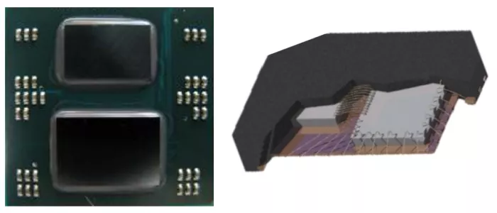
Figure 4: Conventional Flip Chip and Wirebond Multi-Chip Packaging
As transistor scaling according to Moore’s Law slows, chiplets are considered to be one way to extend the transistor density trend through packaging technology. Chiplet interfaces and packaging choices are linked by bandwidth and performance requirements. As interconnect bandwidths and densities are pushed to accommodate massive data transfer rates, the packaging technology to connect chiplets is becoming more sophisticated, even moving into the realm of back-end semiconductor wafer processing.
Understandably, the chiplet packaging cost scales with bandwidth and performance capabilities. Higher data rate capability requires higher interconnect density. Standard chiplet interfaces assume a number of parameters that directly translate to packaging needs:
- Bump pitch and escape pitch → dictates via pad, L/S dimensions
- Depths of signal bumps → Number of layers (including ground planes)
- Acceptable insertion loss → dielectric material choice
- Maximum distance between chiplets
Based on system requirements, a suitable packaging technology meeting performance and cost specifications can be explored. Common options include organic substrates, Fan-Out, Embedded Bridge, Silicon Interposer, and 3D hybrid bonding, which are further detailed in the Appendix.
Table 2 shows a summary of heterogeneous integration packaging technologies, some key attributes, and relative cost. Additionally, other system parameters such as thermal requirements and total system size need to be considered. 2D configurations offer opportunities to isolate higher power, “hot” processor chips from potentially temperature sensitive memory devices, at the cost of larger package size. 3D configurations enable smaller packages.
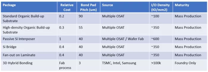
Table 2: Package Technology Relative Cost and Attributes [20]
First-Level Interconnect – The Key to Chiplet Assembly
Packaging methods for integrating multiple semiconductor dice, or chiplets, are defined largely by the first-level interconnect, meaning the initial connection between the chip and a first interposer or substrate. The interconnect density, or connections per area at this first-level has implications with respect to signal bandwidth and integrity, chip area, and packaging cost. In a presentation to IEEE EPS Binghamton Chapter, Lau [19] describes semiconductor packaging technologies ranging from conventional single-chip-on-substrate to 3D stacking of chips, with those technologies in-between utilizing various forms of bridge or interposer options (Figure 5). Conventional packaging methods utilize the package substrate for 1st level interconnects. Advanced packaging utilizes some type of fine-pitch bridge or interposer for these connections.
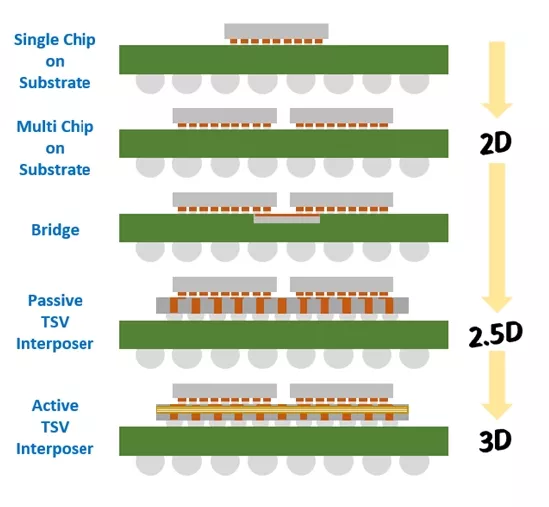
Figure 5: Semiconductor Packaging Technologies
Package Technology Application to Chiplet Interfaces
Chiplet interface standards span a range of performance and bandwidth requirements, see Section 3. Today, packaging technologies are available to accommodate the many existing standards and those in development (Figure 6). As bandwidth increases, the interconnect density grows, leading to I/O pitch reduction. Fitting more I/O in a small area can be achieved by reducing I/O pitch, increasing interconnect routing density or a combination of both. I/O pitch is influenced by the size of the I/O cells (which has implications of ESD protection), the bonding technology, and the amount of signal escape that occurs in-between I/O pads. The interconnect routing density is affected by the number of routing layers, line and space widths in each layer, and the diameter of the vias connecting the routing layers. More layers and finer features equate to higher interconnect density, but not without a price. Figure 7 shows approximate I/O pitch capability relative cost of packaging technologies discussed in this paper based on various published sources. Interface selection and package technology must consider required bandwidth, expansion and extension capability, and product selling price.
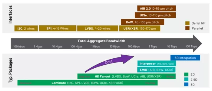
Figure 6: Chiplet Interfaces, Bandwidth and Typical Packages.
Both BoW and UCIe chiplet interfaces offer lower bandwidth interfaces with I/O pitches greater than 100 μm, and higher bandwidth versions with I/O pitches less than 50 μm. High density Interconnect (HDI) substrates and sometimes laminate technology can accommodate greater than 100 μm pitch. The layer count will be determined by signal integrity needs, bonding technology (bond-on-pad vs. bond-on-trace), feature sizes (lines, spacing, vias) and the signal referencing scheme utilized (microstrip vs. stripline). BoW and UCIe reference designs have been demonstrated in substrates ranging from 6 to 10 layers. Coreless substrate designs with fewer layers are likely possible. Cost and performance trade-offs need to be considered for optimal performance at the application price point.
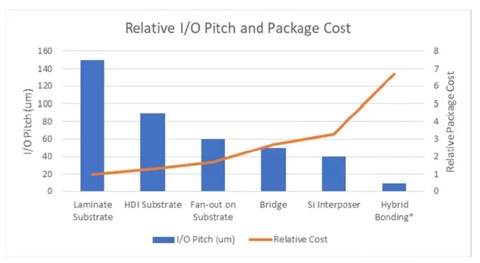
Figure 7: Approximate I/O Pitch and Relative Package Cost (Laminate substrate = 1) for Chiplet Integration Technologies. *Hybrid bonding is done in the wafer fab.
For the interfaces with I/O pitches less than 50um, fan-out (RDL), bridge or interposer technologies are typically needed along with the cost that goes with them, however HDI organic substrate technology has been pushed to I/O pitches substantially lower than 100um. These higher bandwidth interfaces are best suited for products with higher average selling price (ASP).
As wafer fab integration processes such as TSVs (Through Silicon Vias) and hybrid bonding become more mature, the price point drops for using these technologies for chiplet integration. AMD recently announced the Ryzen 5 7600X at a selling price of $299 [21]. This product includes both TSVs and Cu-to-Cu hybrid bonding.
As integration of functions in the package displaces discrete components on the PC board, the product price and package value would understandably increase, opening the door for more advanced and costly packaging technologies. At the same time, as the advanced technologies become more mature and available, presumably the cost will come down. A key component will be establishing interconnect standards and roadmaps which align with the various market segments and price points where chiplets are leveraged.
5. Test and Probe
Testability
The two fundamental reasons for testing semiconductor dies are a) Increase in the quality that directly governs the reliability of the end product and b) Reduce the cost by catching failing chips early. The Design for Testability (DFT) techniques help achieve these goals at a high benefit/cost ratio. In addition, the system reusability of the entire assembly should be taken into consideration. The System DFT approach enables the core/chiplet-level DFT structures to be reused at system level and is critical when the product is deployed in the field for remote diagnosis and data collection.
At chip/chiplet level, DFT are available based on At-speed Scan and Automatic Test Pattern Generation (ATPG), Memory Built-in Self Test (BIST), Logic BIST, Core Wrappers (IEEE 1500), iJTAG (IEEE 1687) and boundary scan (IEEE 1149.X). The cost is an important criterion that governs trade-off when and where to apply these techniques. IEEE 1838, the test standard for 2.5D and 3D packages is playing a crucial role in detecting manufacturing faults in vertical interconnections, especially TSVs [22]. An example of an IEEE 1838 compliant die stack is shown in Figure 8. In such cases, for SiP level testability the constituent chiplets need to be compliant with IEEE 1838 Test Access Architecture for 3D Stacked ICs.
The target test cost is not to exceed 20% of die cost as a rule of thumb from a well-known IC manufacturer with foundry investment. The expectation is the reduced test cost percentage as we go up the hierarchy to package and system level testing.
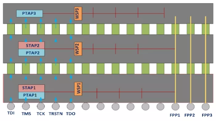
Figure 8: An example of IEEE Standard 1838-compliant stack with serial & parallel data paths.
PTAP: primary test access port; STAP: secondary TAP; FPP: flexible parallel port. WSP:wrapper serial port [22].
Economics
High quality and cost-effective SiP (Systems in Package) production depends directly on the use of chiplets that are designed with reusable test techniques and fault diagnosis as critical design requirements. This requirement can be fulfilled by integrating DFT features during the design phase and utilizing them effectively at different levels of testing. Various test techniques are used in silicon manufacturing steps and they come with different test times and required equipment.
Required test time (for typical structural testing using ATPG) is equal to the product of # of scan patterns, scan chain length and the scan shift frequency. This equation governs the test cost which is reduced by modern DFT techniques that allow increasing shift frequency (Using pipelining) and reducing the scan chain lengths (Using Test Compression)
Testing not only needs the accuracy of the test result but also how quickly you can complete the test. The Economics of Test is governed directly by the Time and Budget available at each level described below.
Wafer/Die Level test requires wafer probe testing. Wafer is diced into individual chips which get tested again after packaging. This is known as Known Good Die (KGD) in case bare die is directly used on the substrate in the case of homogeneous or heterogeneous integration. KGD is an important element in SIP due to its sensitivity to SIP’s gross margin, as illustrated in Figure 9 [23].
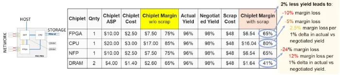
Figure 9: SIP Gross margin sensitivity to changes in KGD level [23].
Module level test (either homogeneous or heterogeneous in case of SiP) requires each constituent chiplet is tested again after assembly, This requires enabling the retargeted tests of each die/chiplet from the top (Module) level controller in one test session. Another test session is enabled to test inter-die connections. The number of test sessions required to complete module level test is directly proportional to the number of chiplets packaged in the SiP as shown in Figure 10. In addition, this also governs the test time to complete the module level test, hence the test cost. Parallel testing of multiple chiplets whenever permissible with architectural hooks and within power directly reduces the final test cost.
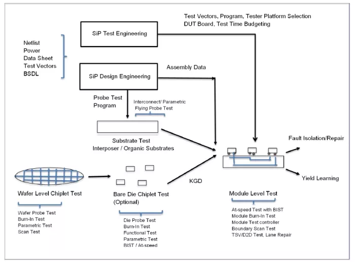
Figure 10: Integrated SiP Production Test flow
6. Chiplet Cost Structure
Deciding between a chiplet design vs monolithic design comes down to cost and return of investment. This chapter first discusses the fundamental cost structure comparison of chiplets versus monolithic design, and then describes three distinct advantages of chiplet design (yield, mixed process nodes, faster time to market) in more detail.
The cost of selling semiconductor products can be split into up-front non-recurring engineering expenses and the full factory cost (FFC) of each product sold. Using a monolithic design as a baseline, the Non-Recurring Engineering (NRE) cost of chiplet development often tends to be lower, see Figure 11. This is because the actual chip development cost can be reduced by (1) designing a family of N products with a smaller number of chiplets, (2) reusing existing chiplets for a previous generation, or (3) leveraging a more mature process node for some chiplets that are easier to design. The mask cost can be higher or lower. It will be higher if only one monolithic product is replaced by a system of several different chiplets. However, the average mask cost per product is less if (1) the chiplet system consists of only one unique chiplet that can be tiled several times or (2) the number of products realized is larger than the number of base chiplets.
The FFC cost with respect to a monolithic system depends on the specific use-case, see Figure 11. Opposing influences may push the cost of silicon higher or lower. It may increase because the overall silicon area of a chiplet system is larger than a monolithic counterpart due to area overhead of the D2D interfaces and other infrastructure like duplicated clocks. However, the smaller size of chiplets results in (substantially) higher die yield and lowers cost/mm2. The probe cost of chiplet systems tends to be higher because each chiplet needs to be probed rather than one monolithic die. Lastly, the packaging cost of chiplet systems is higher since the die-to-die connectivity requires more complex packages (more layers or more advanced package type) to handle the additional die-to-die connectivity.
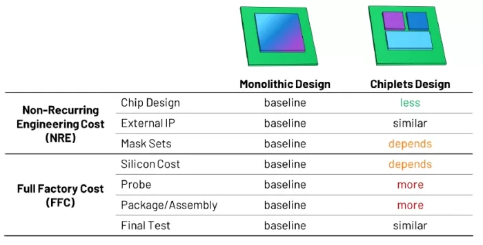
Figure 11: Comparison of costs for monolithic and chiplet-based systems.
Yield-Based Cost Savings
In 2022, the ODSA business group led an effort to develop an open-source chiplet cost model [23-26]. This calculator is an easy way to show that chiplet systems are cheaper to build than monolithic systems in the case of large die on cutting-edge process nodes. This is primarily due to the improved yield at smaller die size and the high wafer cost which is enough to compensate for higher test and package cost. This finding is well reflected in the release of numerous chiplet-based systems in the high-performance computing space where average sales prices are in the hundreds to thousands of dollars and the above as conditions hold true [27-43]. Other cost models, e.g. proposed by Graening et.al [44], come to similar conclusions and further derive the optimal chiplet size depending on constraints.
Process Technology Advantage
The use of chiplets also allows for cost savings by mixing different process technologies in a system. As highlighted in Figure 12 by IBS and referenced in the IEEE Heterogeneous Integration Roadmap, the cost of design varies significantly across different process nodes. The trend is one of exponential cost growth when employing the most recent process nodes, which is partially due to the more complex nature of more advanced nodes. Thus, to offer competitive pricing against single-die SoCs, a viable strategy is to increasingly leverage older process technologies for parts of the system that don’t benefit from the move to a smaller node. This shift could potentially balance performance requirements with cost-effectiveness, optimizing the overall value proposition. To achieve this goal, an efficient system partitioning and defined interfaces within the targeted system are needed.
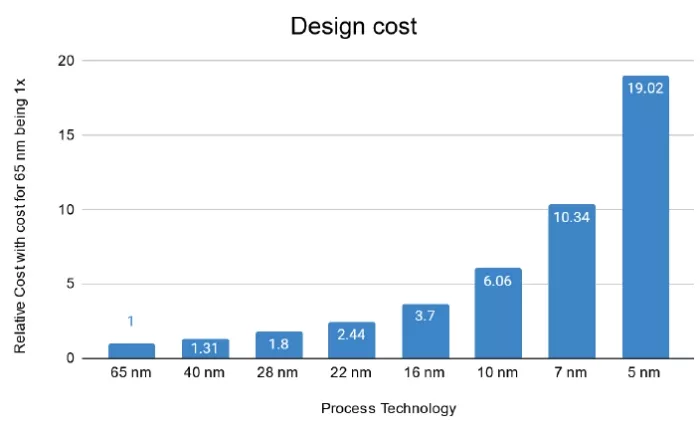
Figure 12: Chip development cost as a function of process node, adapted from [45].
Faster Time to Market through Chiplet Reuse
Reuse of chiplets either in subsequent product generations or within a product family is an important development cost benefit compared to monolithic system design. The lowered design effort often directly translates to a faster product time to market, which improves the return on investment in the following ways:
- Higher market share due to first mover advantage
- Longer product life-cycle results in more units sold
- Higher profit margin
Chiplets can enable an average faster time to market in two ways: as a set of chiplets to build a product family or through the reuse of existing chiplets from previous generations. In the former scenario, a small set of base chiplets can be designed to enable a large number of product versions which would take longer to develop if they were each developed independently. The latter scenario effectively leads to a smaller scale development of a new product, since only part of it, say 1 new chiplet, has to be developed from scratch rather than the whole system.
The financial benefit of a faster time to market can be hard to quantify, since it depends on many factors such as competitor offerings, market dynamics, and product lifecycle. One way to measure the financial impact is to draft two market projections based on a typical and accelerated product release date and take the difference between these two revenue curves. The likely increase in revenue can be weighed against the possibly larger development costs of a chiplet solution or to justify a slightly higher unit cost, say because of higher packaging costs, see Figure 13. Another way, to evaluate the benefit of faster TTM, is to look at the cost of product delay. A classic McKinsey study for example found that a 6-month product delay can cost up to 33% of post-tax profits, whereas a 50% higher development cost with a timely release only results in losses of 3.5%. The aspect of faster TTM or product delays is covered by many articles and books covering [46-49] .
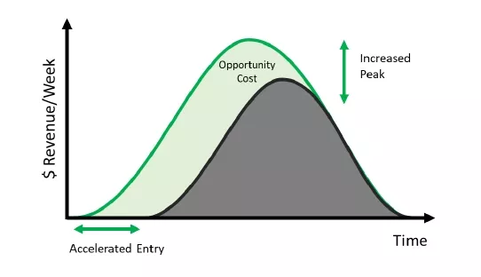
Figure 13 : Increased revenue potential caused by an accelerated product start.
7. Open Chiplet Marketplace
The economics of chiplets are compelling as the market hits the limits of Moore's Law especially in high performance applications. Today the vast majority of leading-edge CPUs, GPUs, AI devices, switches, FPGAs are using chiplets due to their excellent ROI. Die costs can be reduced due to using multi-die versus a large single die, and large integrated vendors develop entire products using the same die to die interface on both sides of the interface. In these current use cases interoperability is a non-issue. With the advent of open standards such as BOW and UCIe becoming available there is the promise (and hope) of an open chiplet market where a designer can purchase off the shelf chiplets to build a custom device or reduce their system development time by partially leveraging external chiplets. For the open chiplet market to work and thrive several issues need to be addressed and will discuss these in this section.
Interoperability & Security are critical to future Adoption
Traditional interconnects such as PCIe, USB, Ethernet have a good validation infrastructure - Verification IP is mature, standards bodies enable interop testing, test equipment companies exist to sell standard specific test hardware. In addition, customers can purchase samples and do their own testing by purchasing reference design boards from vendors - so there is a robust validation ecosystem.
This infrastructure is not yet in place for chiplet interoperability testing. Current usage of chiplets is often limited to closed systems where the chiplets are not sold individually but as part of an overall packaged SiP. Interoperability to standards is not a barrier to adoption in closed systems and chiplets use has flourished for this use case. There is general agreement that standardization is critical to wider chiplet adoption and die-to-die standards are not working on solving these issues. And die-to-die standards alone are not sufficient, test equipment and interop standards will also be needed.
Chiplet interfaces like BoW or UCIe are evolving to address interoperability. In the BoW Link layer 1.0 specification [50], for example, interface profiles help define a complete system interface and aid interoperability through selecting common interface profiles between two chiplets. In UCIe, system-level interoperability is achieved through support for PCIe and CXL protocols if supported by a chiplet. Additionally, the UCIe 1.1 spec adds the concept of a golden chiplet die [51], to aid developers and designers to have confidence in chiplets interoperability.
In the near term, we are seeing islands of interoperability where groups of companies/partners are developing interoperable solutions. It is an important development as the standards solidify and use of golden chiplets we can expect more and more inter-chiplet validation.
Bridge chiplets (PHY, Link) due to inevitable bugs - interface issues
Both main standards for UCIe and BoW are likely to evolve as the industry develops and as companies develop chiplets to be sold on an open market (which will cost millions of dollars) it will be helpful to maximize each chiplets addressable market. It is likely conversion chiplets may be developed to bridge between standards, packaging options as well as fix bugs. One possible path could be FPGA’s that could be used for this function as well where they can play an interim role, such as a recently announced an FPGA chiplet by Quicklogic and YorChip with support for UCIe and BOW, see Figure 14, which could also be used as a bridge between the two interfaces [52]. We anticipate future availability of golden die chiplets which will enable customers to assure interoperability across their system needs. FPGA chiplets can be used to validate interop, validate link layer issues and also help secure the chiplets in production.
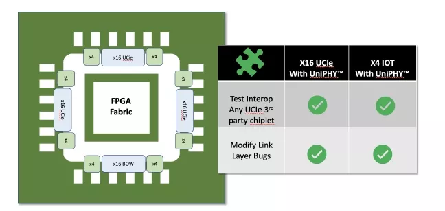
Figure 14: Illustration of proposed FPGA with UCIe and BoW interface.
Supply Chain (e.g. packaging, distribution, KGD)
Packaging is a complex issue and a major barrier for chiplet adoption. The reality is advanced packaging options have limited availability, lead times, costs, yields, etc., are hard to get for smaller companies to even scope out their projects, see Section 4.
Device Qualification and Quality - there are limited standards on this as chiplets are part of an eventual product involving multiple vendor chiplets. We expect early adopters of open chiplet Markets will need to be larger companies with significant in-house design and manufacturing expertise.
Distribution of Chiplets - as the overall industry is just starting out we expect chiplet vendors to team up with other partners to create ecosystems to ease adoption. Currently, large integrated semiconductor vendors have not focused on selling individual chiplets so the open market distribution system is in a very early state.
Know Good Die - once a die has been probed at wafer level it is considered a known good die - and then it will be packaged and undergo final test. In the open chiplet market this is problematic as these chiplets may get damaged in handling, and final packaging involves assembling all multi-vendor chiplets and then performing a final test. Some companies are working on solutions for testing prior to final assembly and hopefully, these solutions will become available as the market evolves.
Return of Investment - entry costs, leadtimes & NRE to deploy chiplets at Scale
For customers and integrators, there will be a significant opportunity to purchase known good die and develop new chiplet based system products. For those customers evaluating purchasing KGD and looking to develop such products - it’s important to understand the integration flow required and requisite expertise:
- Expert System Design Staff: Need to train or hire new staff
- Package Design Expertise and experience: including SI/PI and Power expertise
- Test Program Development: for packaged device including System-Level Test
The costs and time required will likely be substantial - but chiplet based systems will be successful if they can deliver smaller area, smaller power and lower overall cost.
8. Chiplet Design Standardization
For chiplet-based designs to succeed at scale and as an open marketplace, chiplet vendors must be able to provide standard design models that allow their chiplets to be integrated into larger System-in-Package (SiP) designs using electronic design automation tools. Chiplet-based design workflows must consider the most constrained chiplet's requirements, such as fine pitch. Mixing interface standard models with mismatched pitches with bridge die such as Embedded Multi-die Interconnect Bridge (EMIB), adds cost. The proper chiplet interface selection, as discussed in Section 3, will affect which chiplets a system can utilize.
Standardization of Chiplet Models for Heterogeneous Integration
The Chiplet Design Exchange (CDX) workstream proposes a set of standardized chiplet models [53] that should be delivered by chiplet providers to facilitate easy integration into system-level designs from system design to debug and test. Key models include thermal, physical and mechanical, behavioral, power, signal integrity, electrical, test, and security models, as well as the documentation and guidelines as follows:
- Thermal modeling: ECXML format defined in JEDEC JEP181 is recommended. This includes a 3D chiplet description, material properties, and power maps. Time-based power profiles may also be included.
- Physical models: LEF file defining 2D layout views and net information. A GDSII/OASIS file with geometric information is also recommended. A SPICE netlist defines connectivity. Properties like dimensions and tolerances can be captured in JEP30-P101.
- Functional (behavioral) models: Simulation of chiplet functionality. SystemVerilog is recommended, with Verilog-AMS also suggested for analog designs. SystemC models could also be used at a higher system level. Bus Functional Models may also be provided.
- Power models: Estimate chiplet power. Liberty format power libraries and IEEE 2416 standard power models are suggested. UPF/CPF formats can capture power domains/supplies.
- Signal integrity analysis: IBIS/IBIS-AMI models of I/O buffers. Optional SPICE netlists or channel models may also be included.
- Power integrity analysis: Chip Power Models (CPM) is utilized in capturing on-chip RLC parasitics.
- Test models: Boundary scan (BSDL), JTAG (IJTAG), ATPG patterns, and BIST vectors.
- Documentation: Chiplet information, SiP integration guidelines, test guides, and optional security/firmware data.
A standardized baseline for chiplet models will help enable scalable, heterogeneous chiplet-based system design through an open vendor ecosystem and chiplet marketplace. Adoption of these model recommendations could significantly help advance next-generation computing architectures leveraging hybrid chip integration approaches.
Open Standard Format for Chiplet Data Exchange
Using an open standard format for chiplet data, such as the OCP/CDXML-JEDEC/JEP30 integrated chiplet standard format would help reduce friction of the development and boost the economy of chiplet-based design. CDXML [54] is developed under OCP and is being integrated into the JEDEC/JEP30 Part Model [55]. CDXML consists of an XML schema, and the structure of the chiplet standard format defines the mechanical, IO, electrical, and assembly properties of a chiplet. CDXML also includes the CDK checklists for the standardized chiplet models defined in the previous section. An open standard format offers the following benefits:
- Interoperability: Standard chiplet data formats enable interoperability among chiplet providers, design tools, and manufacturing processes, ensuring seamless communication and compatibility. This is achieved through common standards for physical interfaces like SerDes lanes, data rates, and protocols, such as UCIe and BOW.
- Design Reusability: Chiplet designs become reusable, saving time and effort, thanks to standard data formats. Designers can easily share and integrate chiplets into their designs without compatibility concerns.
- Design Tool Integration: Integration with Electronic Design Automation (EDA) software becomes smoother, enabling collaboration between design teams and tools.
- Design Verification: Accurate design verification and simulation are facilitated, reducing manufacturing errors and iterations.
- Design Analysis: Efficient analysis of chiplet designs, including signal integrity, power, thermal, and electromagnetic compatibility, is possible with standard data formats.
- Simulation and Modeling: System-level simulations with chiplet designs become comprehensive, validating functionality and behavior under various conditions without physical prototypes.
- Testability and Test Coverage: Testability and test coverage improve with standardized data formats, helping develop effective test strategies of 3rd party chiplets and ensuring better integration into the overall test infrastructure.
- Fault Diagnosis and Debugging: In case of failures, fault diagnosis and debugging are expedited with standardized chiplet models, enhancing product quality and reducing time-to-market.
- Design for Test (DFT): Design for Test (DFT) features, such as scan chains and BIST, integrate seamlessly into chiplet designs with standard data exchange formats, simplifying DFT implementation and testing.
- Testability and Test Coverage: Compliance testing becomes more straightforward as standardized data formats facilitate sharing design representations with testing bodies, streamlining verification.
- Supply Chain Flexibility: Supply chain flexibility is enhanced by selecting chiplets from various suppliers, promoting competition, and potentially reducing costs.
- Scalability: Scalability of complex systems is enabled with chiplet-based designs, and standard data formats ensure easy integration, replacement, or upgrades.
- Ecosystem Development: Adopting a standard format fosters an open chiplet ecosystem, encouraging collaboration, innovation, and best practices sharing among designers, manufacturers, and users, leading to a wider variety of chiplet options and improved system capabilities.
By leveraging a standard data format in chiplet-based design, designers can enhance analysis capabilities, streamline testing processes, improve test coverage, enable efficient fault diagnosis and debugging, facilitate DFT implementation, and simplify compliance testing. This analysis and testing benefits contribute to higher-quality designs, reduced risk, and improved overall reliability of chiplet-based systems.
Standardized Integration Workflows for Heterogeneous Chiplet Systems
Proper planning and understanding of integration workflows is essential for businesses to leverage chiplets effectively. CDX proposed a guide to integration workflows for heterogeneous chiplet systems [56] outlines detailed workflows for various stages of chiplet design and integration like partitioning, architectural planning, simulation, verification, physical design, power/thermal analysis, testing, etc. Understanding these workflows can help evaluate the engineering efforts and costs involved in developing a chiplet-based system.
- Physical planning workflows provide insights into die size requirements, chiplet placement constraints, etc. This data can be leveraged to estimate chip manufacturing and assembly costs.
- Functional simulation and verification workflows can be used to estimate chiplet verification and validation times, which have a significant impact on development costs and timelines.
- Power planning and analysis workflow gives insights into power delivery requirements, rail segmentation needs, on-chip/off-chip decoupling capacitance estimation etc. This helps evaluate power infrastructure costs.
- Thermal modeling workflows indicate cooling solution needs - active/passive, liquid/air etc. This assists in estimating thermal management system costs.
- Mechanical analysis workflow aids evaluation of packaging and assembly costs for heterogeneous chiplets with different process technologies.
- Testing workflows outline multi-chiplet qualification and reliability testing procedures. This gives an idea of additional testing costs for chiplet-based designs over monolithic designs.
These detailed workflows enable accurate forecasting of engineering resources, timelines, costs related to NRE development, EDA tools, prototyping, packaging and testing. With visibility into the technical execution complexities, organizations can effectively evaluate the chiplet technology and business case to optimize returns on their chiplet-focused investments and commercialization plans.
9. Conclusion and Next Steps
Chiplets are a promising design philosophy to lower product development and unit costs and increase product time-to-market. To determine whether a chiplet-based architecture is beneficial it is essential to understand the interplay between system design and technology options. Existing chiplet whitepaper describe the benefits of chiplets but insufficiently explain this linkage of design trade-offs and financial analysis in cases where full factory cost improvements alone are not enough to justify chiplets. This whitepaper presents a holistic view of chiplet technology options and business considerations. It enables case studies of chiplet-based designs addressing both internal chiplet design and an emerging external chiplet market.
To start a new case study, it is helpful to describe the desired system at a high level and sketch out derivative options or possible chiplet reuse opportunities scenarios. Chapter 2 highlights the two main ways this can be done with homogeneous or heterogeneous system architecture. The former uses the same process node for all chiplets and is often used for yield enhancement and large compute systems, while the latter implies chiplets in different process nodes and is employed to optimize cost and increase system performance.
Die-to-Die (D2D) interfaces create the connections between chiplet to build larger systems. Chapter 3 outlines how to pick a D2D interface based on clear metrics and compares four chiplet interfaces (AIB, BoW, UCIe, XSR) that are popular today. The next few years will likely paint a clearer picture of which standards will prevail with growing ecosystems and we will see definitions of 3D chiplet interfaces.
D2D interfaces are closely linked to packaging technology required to implement this connection. Chapter 4 illustrates the common packaging options for chiplets systems ranging from in-expensive prepreg substrates for lower-throughput to high-performance and higher cost organic or silicon interposer. The both limited availability and high price of advanced packaging options will likely resolve as these high-end packages become mainstream in the future.
Building chiplet systems in an economical way requires the use of test insertions at different points in the production flow to minimize scrap cost. Chapter 5 reviews common design for test features from 2D to 3D systems and describes the underlying economics of test steps such as wafer probe, substrate test, final and system level test. More standardization of design for test features will hopefully materialize in the future to streamline easy re-testing of 3rd party die.
Having discussed the key design choices and cost contributors, it is now possible to project the financial feasibility of a chiplet design based on non-recurring engineering costs (NRE) and full factory costs. Chapter 6 summarizes the chiplet cost structure and points out differences to monolithic design. It also provides additional detail on the three possible cost advantages of chiplets design based on improved yield from smaller die, lower design and wafer cost from older process nodes and higher return from a faster timer to market.
Future system designers will be able to choose from internally developed chiplets and externally available die from 3rd parties. Chapter 7 describes challenges and next steps to enable this chiplet marketplace. Additionally, standardization will play a key role to create a flourishing and open chiplet economy. Chapter 8 discusses several contributions from the ODSA Chiplet Design Exchange group that has released reference documents for chiplet models, data formats and integration flows. The adoption of these and other new chiplet standards will be an important marker whether chiplets continue to only be used by large, vertically integrated companies or whether a vibrant and open chiplet economy can emerge.
Chiplets for Prototyping
Beyond chiplets as cost and time to market optimized product strategies, this concept is interesting for prototyping even if the final system may eventually be a monolithic design. The challenges of creating a chiplet ecosystem are significant both from the business and technical perspectives and they likely all need to be addressed simultaneously. This challenge can seem very daunting. A potential way around this would be to consciously devise an organic, boot strapped, top down, chiplet enablement strategy for bringing chiplet solutions to the market, which is in contrast to the current Bottom-Up efforts taking place at the moment [57].
To create a chiplet-based SoC for a specific application, we could follow these steps:
- Simulate the complete SoC in software.
- Partition the simulation into chipletized parts.
- Leverage simulation IP from chiplet providers.
- Target chiplet designs to an FPGA-based SoC emulation platform.
- Integrate available real chiplets with a Chiplet-to-Emulation bridge chiplet.
- Achieve Hardware-In-The-Loop (HWIL) with real chiplets in the emulation loop.
- Gradually replace emulation parts with real chiplets as they become available.
- The final module will represent the completed SoC with all chiplets.
- The module is designed for deployment in a real compute infrastructure.
- This enables a path to run applications in software simulation to the final chiplet assembly.
Chipletized solutions provide a low-cost route to market for low-volume products, potentially transitioning to a monolithic solution as demand grows. ASIC IP vendors could generate earlier revenue by selling IP as chiplets before licensing it for monolithic integration.
10. References
[1] Hackenberg, Tom. Chiplet Market Update. Chiplet Summit, 2023
[2] Insights, M. T. R. (2023, September 15). Multi-die systems define the future of semiconductors.
[3] Park, J. (n.d.). Chiplets and Heterogeneous Packaging Are Changing System Design and Analysis. Cadence.com. Retrieved December 14, 2023
[4] Park, J. (2023, February 1). HETEROGENEOUS INTEGRATION - CHIPLETS. Expedera. Retrieved December 14, 2023
[5] S. Naffziger et al., "Pioneering Chiplet Technology and Design for the AMD EPYC™ and Ryzen™ Processor Families : Industrial Product," 2021 ACM/IEEE 48th Annual International Symposium on Computer Architecture (ISCA), Valencia, Spain, 2021, pp. 57-70, doi: 10.1109/ISCA52012.2021.00014.
[6] Semiconductor Engineering. (2023, August 7). Chiplets: Deep Dive Into Designing, Manufacturing, And Testing. www.Semiengineering.com. Retrieved December 14, 2023
[7] Siemens EDA. Heterogeneous chiplet design and integration: Bringing a new twist to SiP design. www.Siemens.com. Retrieved December 14, 2023
[8] Hempel, Marek. ODSA Chiplet Business Challenges - Summary Presentation. ODSA General Meeting, March 2023
[9] Saban, K. (n.d.). Xilinx Stacked Silicon Interconnect Technology Delivers Breakthrough FPGA Capacity, Bandwidth, and Power Efficiency. Www.Xilinx.com. Retrieved December 14, 2023
[10] S. Ardalan et al., "Bunch of Wires: An Open Die-to-Die Interface," 2020 IEEE Symposium on High-Performance Interconnects (HOTI), Piscataway, NJ, USA, 2020, pp. 9-16, doi: 10.1109/HOTI51249.2020.00017.
[11] UCIe (n.d.). Universal Chiplet Interconnect Express (UCIe)®: Building an open chiplet ecosystem. Www.Uciexpress.org. Retrieved December 14, 2023, from https://www.uciexpress.org/general-8 [12] Cadence (n.d.). 40G UltraLink D2D PHY. Retrieved December 14, 2023
[13] Synopsys (n.d.). Synopsys Die-to-Die IP Solutions. Retrieved December 14, 2023
[14] GUC (n.d.). Die-to-Die (GLink-2.5D/3D) IP. Retrieved December 14, 2023, from
[15] Kandou (n.d.). Glasswing® GW12-500-USR. Retrieved December 14, 2023
[16] OIF (n.d.). 112 Gbps Electrical Interfaces An OIF Update on CEI-112G. Retrieved December 14, 2023
[17] ODSA (n.d.). Inter-chiplet options_2020_release. Www.Opencompute.org. Retrieved December 14, 2023
[18] Leibson, S. (2023, August 21). Intel’s Chiplet Strategy Accelerates FPGA Development. www.Forbes.com. Retrieved December 14, 2023
[19] John H Lau; Unimicron Technology Corporation; “Recent Advances and Trends in Advanced Packaging”; IEEE EPS Binghamton Chapter; April 13, 2022
[20] Jan Vardaman, Tech Search Inc. 2022
[22] Alcorn, P. (2021, August 23). AMD Unveils More Ryzen 3D Packaging and V-Cache Details at Hot Chips. Retrieved December 14, 2023
[22] Adom Cron, Erik Marinissen; Synopsys; “IEEE Standard 1838 is on the move”; Computer Vol. 54, no. 11, 2021
[23] Open Compute Project (n.d.). DEVELOPING AN OPEN CHIPLETS MARKETPLACE: CHALLENGES AND OPPORTUNITIES. Opencompute.org. Retrieved December 14, 2023 This work is licensed under a Creative Commons Attribution-ShareAlike 4.0 International License. PAGE 29
[24] M. Ahmad, J. DeLaCruz and A. Ramamurthy, "Heterogeneous Integration of Chiplets: Cost and Yield Tradeoff Analysis," 2022 23rd International Conference on Thermal, Mechanical and Multi-Physics Simulation and Experiments in Microelectronics and Microsystems (EuroSimE), St Julian, Malta, 2022, pp. 1-9, doi: 10.1109/EuroSimE54907.2022.9758914
[25] (n.d.). OS Chiplet Cost Model v18_VH ODSA BWG. ODSA. Retrieved December 14, 2023
[26] Ahmad, M. (2022, March 24). To Chiplet or Not To Chiplet: Heterogeneous Integration and Chiplets. IEEE. Retrieved December 14, 2023
[27] (n.d.). Chiplet Architecture Accelerates Delivery of Industry-Leading FPGA Features and Capabilities . Intel.com. Retrieved December 14, 2023
[28] (n.d.). Intel's Ponte Vecchio is Finally in The Wild. Tom's Hardware. Retrieved December 14, 2023
[29] (n.d.). Ntel will launch Meteor Lake on December 14th — This is Intel’s Core Ultra. The Verge. Retrieved December 14, 2023
[30] (n.d.). Sapphire Rapids Is A Critical Turning Point For Intel. Forbes. Retrieved December 14, 2023
[31] (n.d.). Virtex UltraScale+ VU19P FPGA Highest capacity FPGA now in production by AMD. Xilinx. Retrieved December 14, 2023
[32] (n.d.). AMD Instinct MI300 Data Center APU Pictured Up Close: 13 Chiplets, 146 Billion Transistors. Tom's Hardware. Retrieved December 14, 2023
[33] (n.d.). AMD RDNA 3 GPU Architecture Deep Dive: The Ryzen Moment for GPUs. Tom's Hardware. Retrieved December 15, 2023, This work is licensed under a Creative Commons Attribution-ShareAlike 4.0 International License. PAGE 30
[34] Marvell (n.d.). What’s Next in System Integration and Packaging? New Approaches to Networking and Cloud Data Center Chip Design. Retrieved December 15, 2023
[35] Marvell (n.d.). Custom ASICs. Retrieved December 15, 2023, from
[36] WCCFTECH (n.d.). NVIDIA’s Next-Gen Blackwell GB100 GPUs Utilize Chiplet Design, Feature Significant Changes. WCCFTech. Retrieved December 15, 2023
[37] Anandtech (n.d.). Nvidia Anounces A10 -80GB Ampere Gets HBM2e Memory Upgrade. Retrieved December 15, 2023
[38] Nvidia (n.d.). NVIDIA Hopper Architecture In-Depth. Retrieved December 15, 2023
[39] Semianalysis (n.d.). Amazon Graviton 3 Uses Chiplets & Advanced Packaging To Commoditize High Performance CPUs | The First PCIe 5.0 And DDR5 Server CPU. Retrieved December 15, 2023
[40] CNET (n.d.). Apple's M1 Ultra Shows the Future of Computer Chips. Retrieved December 15, 2023
[41] Ventana (n.d.). Ventana Introduces Veyron V2 — World’s Highest Performance Data Center-Class RISC-V Processor and Platform. Retrieved December 15, 2023
[42] HPCWire (n.d.). D-Matrix Launches New Platform to Address Growing Compute Demand for Generative AI. Retrieved December 15, 2023
[43] Dream Big Semiconductor (n.d.). Our Products. Retrieved December 15, 2023
[44] A. Graening, S. Pal and P. Gupta, "Chiplets: How Small is too Small?," 2023 60th ACM/IEEE Design Automation Conference (DAC), San Francisco, CA, USA, 2023, pp. 1-6, doi: 10.1109/DAC56929.2023.10247947.
[45] Li, Tao & Hou, Jie & Yan, Jinli & Liu, Rulin & Yang, Hui & Sun, Zhigang. (2020). Chiplet Heterogeneous Integration Technology—Status and Challenges. Electronics. 9. 670. 10.3390/electronics9040670.
[46] Supply & Demand Chain Executive (n.d.). What Are Late Product Launches Really Costing You? Retrieved December 15, 2023
[47] Product Plan (n.d.). Why Cost of Delay is a Product Manager’s Secret Weapon. Retrieved December 15, 2023
[48] UpWork (n.d.). The Surprising Cost of Delayed Product Launches. Retrieved December 15, 2023
[49] TCGen (n.d.). Time To Market (TTM): What it is & Why It’s Important. Retrieved December 15, 2023
[50] OCP (n.d.). Transaction and Link Layer Specification for Bunch of Wires (BoW) Interfaces. Opencompute. Retrieved December 15, 2023
[51] UCIe (n.d.). UCIe™ 1.1 Specification: Backward Compatible Evolution of UCIe for Driving an Open Chiplet Ecosystem with New Usage Models. UCIexpress. Retrieved December 15, 2023
[52] PR News Wire (n.d.). QuickLogic and YorChip Partner to Develop Low-Power, Low-Cost UCIe FPGA Chiplets. Retrieved December 15, 2023
[53] Proposed Standardization of Chiplet Models for Heterogeneous Integration
[54] Chiplet Data Exchange Markup Language
[56] Guide to Integration Workflows for Heterogeneous Chiplet Systems, To be released in the Chiplet Summit 2024
[57] ODSA (n.d.). System Architecture Considerations for Chiplet Enablement. Youtube. Retrieved December 15, 2023
[58] ECO-CHIP: Estimation of Carbon Footprint of Chiplet-based Architectures for Sustainable VLSI (arxiv.org)
12. About Open Compute Foundation
At the core of the Open Compute Project (OCP) is its Community of hyperscale data center operators, joined by telecom and colocation providers and enterprise IT users, working with vendors to develop open innovations that, when embedded in products, are deployed from the cloud to the edge. The OCP Foundation is responsible for fostering and serving the OCP Community to meet the market and shape the future, taking hyperscale led innovations to everyone. Meeting the market is accomplished through open designs and best practices, and with data center facility and IT equipment embedding OCP Community-developed innovations for efficiency, at-scale operations and sustainability. Shaping the future includes investing in strategic initiatives that prepare the IT ecosystem for major changes, such as AI & ML, optics, advanced cooling techniques, and composable silicon. Learn more at www.opencompute.org.
13. Compliance with Open Compute Project Tenets
This whitepaper, authored by the business workstream of the Open Domains Specific Architecture Group, complies with the five tenets of the Open Compute Project as detailed in the paragraphs below.
Openness
Participation in the ODSA and the business workstream is open to everyone. The meeting times are posted online and anyone can join, participate and contribute. The drafts for this whitepaper were hosted online and sent out regularly to anyone signed up for the ODSA mailing list to seek feedback.
Efficiency
The goal of this whitepaper is to address the business challenges of designing chiplet-based systems. Chiplets are a design methodology to build systems out of modular die (chiplets) with standardized interfaces. This allows for chiplets to be reused across different product designs which allows complex systems to be created faster, with less development effort and often with lower unit cost clearly embodying the tenet of efficiency.
Impact
Chiplet technology has a transformative impact on the semiconductor industry. Today, many big companies leverage chiplet technology to achieve the highest levels of performance at manageable design time and cost. We believe this whitepaper is impactful because it will help smaller companies understand the business challenges of chiplets better and reap the benefits of chiplet-based designs.
Scale
Coming up with chiplet-based products is a design philosophy rather than a rule-based classification. As such, the insights described in this whitepaper can be easily scaled to many application areas within semiconductor product design. Additionally, chiplets enable building scalable product portfolios through defining base chiplets that can be defined in various ways to meet different performance, feature and cost targets.
Sustainability
The modular and reusable nature of chiplets makes this design approach more sustainable than repeated custom monolithic designs. This thesis is discussed further for example by a paper by Sudharshan, et. al. on the positive impacts of chiplets on the operational carbon footprint [58]. As a result, we believe this paper is in-line with building a more sustainable semiconductor industry.
14. Appendix
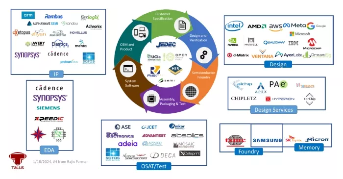
A. List of Chiplet-related Vendors
Designing chiplets requires a whole value chain from design to test and packaging to realize a product development. Below is a partial list of chiplet-related vendors by area that can serve as a starting point for getting the necessary support (based on contributing authors’ knowledge).
B. Chiplet Events
Below is a list of up-coming events that cover chiplet technology.
- OCP Global Summit - Oct 17-19, 2023
- APCS Dec 13-15, 2023
- Chiplet Summit - Feb 6-8, 2024
- OCP Regional Summit - Apr 24-25, 2024
- Hot Chips
- ChipCON
- IMAPS
- ECTC
- DAC
- SemiconWest
- ISSCC
- ISQED.org
- ISPD.cc
- HiPChips
C. Packaging by Category
Organic Substrate Technology
Organic substrates are typically made up of epoxy-glass composites with Cu conductors. The construction of these substrates often resembles that of a PC board. However, the fabrication technique and materials used affect the cost and performance of the final product. The layering of organic substrates can be categorized as either “cored” or “coreless” (Figure 15). A cored substrate has a relatively thick central core, typically made of a glass fiber / epoxy composite. This core serves as the initial substrate on which subsequent routing layers are built, and also provides a certain amount of rigidity beneficial to package and board assembly processes. The additional routing layers can be of similar glass fiber / epoxy composite laminate, or build-up film, commonly referred to a ABF in reference to the major supplier and material used – Ajinomoto Build-up Film. ABF technology offers finer line and space capability compared to laminate and is often referenced as HDI (High Density Interconnect).
Cored substrates have a generally larger via size and pitch because of the need to drill through the thick core. This impacts routing density as well as signal and power integrity. Alternatively, a coreless substrate has only the thinner routing layers. It is fabricated by building the routing layers on a removable carrier. Without the thick core, the negative routing and electrical performance implications of the cored substrate are eliminated. In one process, an “embedded trace” structure is created, which does not require a solder mask to define the bond pads. This is conducive to Cu pillar bond-on-pad without presolder. Coreless technology can often be used for a “layer-down” strategy where, for example, a design requiring 4 layers in cored technology can be routed using only 3 coreless layers. The thinner coreless substrate does however present package assembly handling and warpage challenges which must be considered.
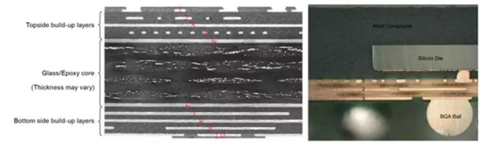
Figure 15: Structure of cored (left) and coreless substrate (right) [Source: NXP]
Fan-Out Technology
Extending wafer-level CSP redistribution layer (RDL) technology to “fan-out” to a larger format has been in production for some time. Chips are placed on a wafer or panel carrier to create a “reconstituted wafer” or panel. Multiple chips and passive devices can be integrated into a single fan-out package. Traditionally, an epoxy mold compound is used to embed the die.
Recently configurations in which the die are embedded in organic laminate or silicon have been developed. Fan-out technology is capable of finer lines and spaces compared to organic substrate technology. Common fan-out processes are either “chip-first” or “chip-last” (Figure 16).
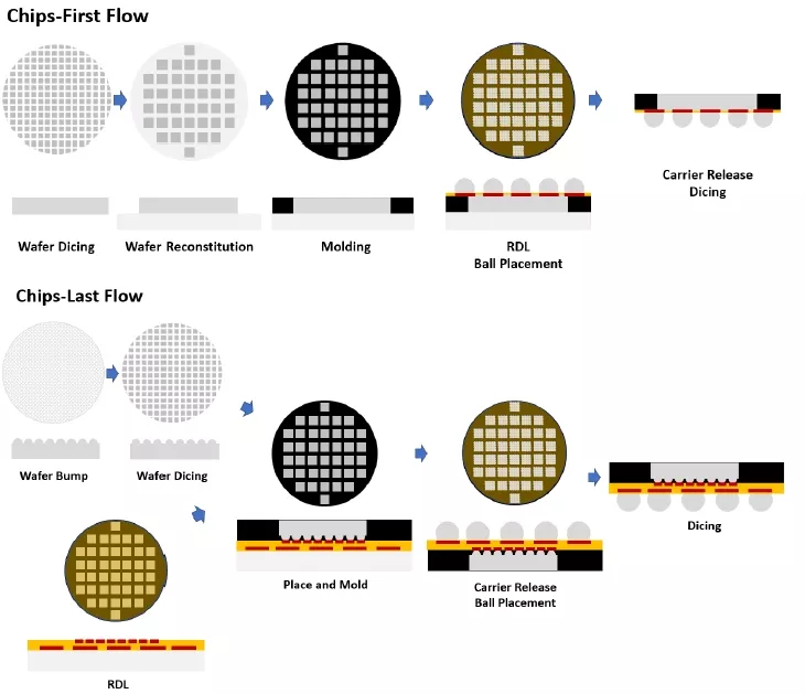
Figure 16: Chip-first (top) and chip-last (bottom) fan out process flows.
In the “chip-first” process, the RDL is built-up on top of the die in the reconstituted wafer or panel, enabling finer I/O pitch compared to chip-last, as tolerances for bumping and placement are not required. The tolerances are influenced by placement accuracy of the chips in the reconstituted media and the lithography process used. Wafer or panel warpage is sometimes a challenge when using the chip-first process for complex multi-chip packaging.
In the chips-last process, the RDL is formed on the carrier first, and then the chips are placed. With this process, known good die (KGD) processing is easier than chips-first since the bumped die are easier to test. While chips-last and chips-first configurations offer similar lines and space capabilities, chips-last will have limitations on die I/O pad pitch dictated by the bump UBM and via size requirements, as well as die placement tolerance.
Fan-out technology typically has a higher cost per area compared to organic substrates, driven primarily by a smaller processing format. As warpage and defectivity reduction advances are made, larger panel formats continue to improve fan-out packaging cost. It has been found that a cost-effective solution is to use one or more fan-out RDL layers to connect the nearby chiplets, and then mounting the RDL package on a large organic substrate for connection to the final application PC board (Figure 17).
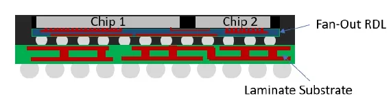
Figure 17. Fan-Out on Substrate
Silicon Interposer
In 2013, Xilinx and TSMC jointly announced the production of Virtex-7 product family which is considered by many to be the first “splitting” of a large chip into smaller pieces for yield reasons, and is claimed to be claimed to be industry’s first heterogeneous 3D ICs in production (Figure 18). This product was the first to use the TSMC CoWoS technology, which combines multiple chips onto a Si interposer featuring TSVs and solder bumps on the bottom to attach to a flip-chip substrate. While the CoWoS package cost adder was significant, the die cost savings realization due to yield improvement made the crossover to chiplets attractive. Since then, others have followed suit with silicon interposer solutions including AMD and NVIDIA (GPU + HBM).
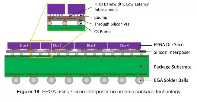
Figure 18. FPGA using silicon interposer on organic package technology.
Embedded Bridge / Chip Technology
Embedded bridge structures create horizontal connections between chiplets in package (Figure 19). The chips are attached on top of a build-up package substrate with the “bridge chip” embedded within. The chiplets must connect to both the organic build up layers, having coarser lines and spaces, as well as the bridge chip with the finer lines and spaces to facilitate high bandwidth communications between the chips. Embedded chip substrate manufacturing is highly specialized and comes at a cost premium due to the complexity of fabricating an organic build-up package substrate with the embedded silicon bridges while still meeting flatness and bond pad location tolerance requirements. Additionally, the process of bumping with two different UBM diameters (standard pitch plus smaller pitch for bridge) is difficult to control as plating rates can vary with UBM diameters, and typically requires a two-step lithography process where one UBM size is first created, followed by the 2nd.
Another method to create the bridge structure is to do the bonding of the chiplets and bridges first, and then attach the assembly to the substrate having a cavity allowing clearance for the bridge chip. This addresses substrate flatness challenges presented by the embedded silicon, and also eliminates the need to include two different UBM diameters on the chiplet, as the pillars to attach the chiplet to substrate are created on the chiplet, and the pillars to connect the bridge to the chiplet are created on the bridge. Bridges can also be embedded in fan-out packages.
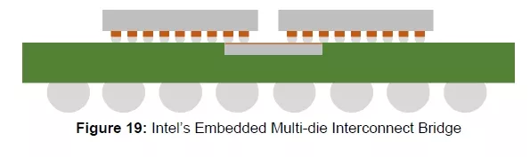
Figure 19: Intel’s Embedded Multi-die Interconnect Bridge
Hybrid bonding, Cu-Cu Bonding
Hybrid bonding combines a dielectric bond with a metal bond. The activated dielectric surfaces are bonded after aligning the wafers or die using optical alignment. This is followed by an anneal to diffuse metal atoms creating the metal bond (Figure 20). Since hybrid bonding is a 3D configuration, die-to-die signal density is dependent upon bond pad pitch. With no soldering required, and using wafer fabrication equipment, bond pad pitches sub 10 μm are possible. Bonding can be wafer-to-wafer if the die to be bonded are the same size, or die-to-wafer if the die are different sizes.
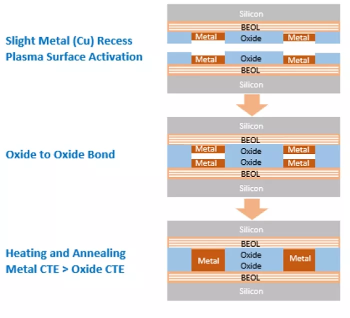
Figure 20: Hybrid Bonding Process Flow
D. Test and Probe
There are various Design for Test (DFT) strategies employed at various levels of microelectronics system integration using chiplets and advanced packaging. We need a way to model how various test strategies such as Stuck-Al Scan Test, At-speed scan test, IDDQ, boundary scan, Memory BIST, Logic BIST impact the full set or subset of the parameters described above. This model will have the ability to take the above listed parameters and various test methods primarily DFT techniques as inputs and will do multi-objective optimization to give an optimal test cost for the final package. The D2D interface will play a very important role in this proposed test model.
| Wafer | Chiplet | D2D Interfaces | System in Package |
| Probe Test | Bare Die Probe | Full Probe | |
| Parametric | On Chip Parametric | Parametric Test | |
| Burn-In | Chip Level Burn-In | Module Burn-in | |
| Wafer level at-speed scan | Stuck-At and At-Speed Scan Test using IEEE 1687 & IEEE 1500 | Loopback Test | At-Speed Scan Test using IEEE 1149.1, IEEE 1838 |
| Memory BIST | Memory BIST | ||
| Boundary Scan | Boundary Scan | ||
| Functional Test | Functional Test | Functional Test |
Table3 : Different Test Techniques at Various Levels of Chiplet Manufacturing.
Related Chiplet
- DPIQ Tx PICs
- IMDD Tx PICs
- Near-Packaged Optics (NPO) Chiplet Solution
- High Performance Droplet
- Interconnect Chiplet
Related Technical Papers
- CATCH: a Cost Analysis Tool for Co-optimization of chiplet-based Heterogeneous systems
- CHICO-Agent: An LLM Agent for the Cross-layer Optimization of 2.5D and 3D Chiplet-based Systems
- Thermal Implications of Non-Uniform Power in BSPDN-Enabled 2.5D/3D Chiplet-based Systems-in-Package using Nanosheet Technology
- Stop-For-Top IP model to replace One-Stop-Shop by 2025... and support the creation of successful Chiplet business
Latest Technical Papers
- Affinity Tailor: Dynamic Locality-Aware Scheduling at Scale
- AMMA: A Multi-Chiplet Memory-Centric Architecture for Low-Latency 1M Context Attention Serving
- Exploring the Efficiency of 3D-Stacked AI Chip Architecture for LLM Inference with Voxel
- Epoxy Composites Reinforced with Long Al₂O₃ Nanowires for Enhanced Thermal Management in Advanced Semiconductor Packaging
- Chipmunq: A Fault-Tolerant Compiler for Chiplet Quantum Architectures