Building Advanced 3D Devices with DBI®
By NHanced Semiconductors
NHanced Semiconductors has used Direct Bond Interconnect (DBI1 ) to assemble 3D integrated circuits for nearly two decades, both die-to-wafer and wafer-to-wafer. Figure 1 shows a crosssection of a stack of 8 active wafers. To date, wafers have been stacked to a height of 20 layers.
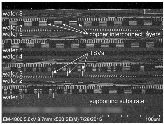
Figure 1: Eight-layer 3D wafer stack with 80 layers of copper wiring; stack height is 160µm
The Benefits of 3D
3D integration reduces circuit footprint and weight. It also reduces interconnect length, thereby reducing power and improving signal speed. Past work has shown 40-90% power reduction and 3-fold to 5-fold latency or speed improvements. An additional benefit is improved security: the many thin layers of circuitry are extremely difficult, if not impossible, to separate and then analyze for function.
DBI® Process Flow
The DBI process uses a two-step kinetic reaction to form silicon oxide bonds followed by annealing to form metalmetal bonds.
The first step directly bonds the two surfaces using van der Waals forces. At room temperature the surfaces – in Figure 2, two wafers – are aligned and brought into contact. Each surface has a naturally adsorbed dipole layer of moisture (water) that initially repels the opposite surface. One layer “floats” above the other until a gentle force, usually a mechanical pin, presses lightly at the edge. This overcomes the electrostatic repulsion and enables the water molecules to bond through van der Waals forces.
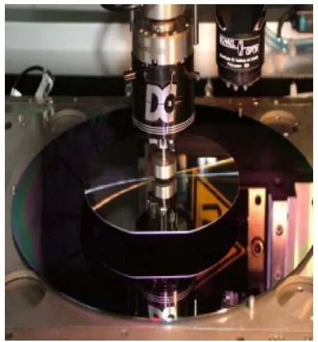
Figure 2: Alignment of wafers
The second step is heating, which forms covalent Si-O-Si bonds (Equation 1 and Figure 3).
Equation 1: Si-OH + Si-OH ---------- Si-O-Si + H2O
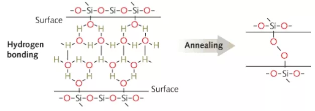
Figure 3: Direct oxide bonding
The high temperature normally required for this reaction is not suitable for 3D IC fabrication. However, modifying the surface chemistry allows the chemical bonds to form at significantly lower temperatures. Various such surface modification technology has been reported and patented. The method we use is to first prepare metal vias or TSVs interconnecting to a surface (via) or backside (TSV) metal. We then deposit oxide, followed by chemo-mechanical polishing to expose the metal/SiO2 coplanar surface. This is a single mask level process if the seed layer used for electroplating is blanket-etched following electroplating. These unit process steps are similar to those used in volume foundry interconnect stack fabrication manufacturing.
Figure 4 illustrates the process flow using copper (Cu) as the DBI metal; using nickel (Ni) employs a slightly different process.
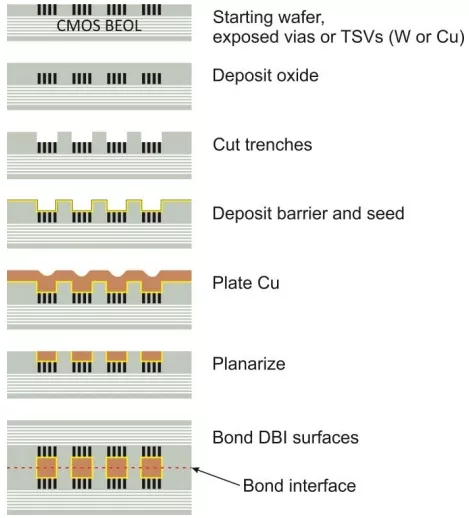
Figure 4: Proprietary DBI process flow using Cu
Subsequent heating of the bonded structures in a standard clean room oven forms a monolithic, low resistance metal-metal interface. The activated and terminated oxide layers are already bonded together with high strength. The metal-metal interface is therefore subject to internal pressure when the metal expands at elevated temperatures. Due to this pressure, a reliable metallic bond results even though the temperature is lower than a standard anneal for that metal. NHanced normally uses 300°C to achieve a low resistance Cu-Cu interface, but the process has been demonstrated successfully at a processing temperature of only 150°C.
1 DBI is a registered trademark of Adeia Inc.
Related Chiplet
- Interconnect Chiplet
- 12nm EURYTION RFK1 - UCIe SP based Ka-Ku Band Chiplet Transceiver
- Bridglets
- Automotive AI Accelerator
- Direct Chiplet Interface
Related Technical Papers
- Intel Delivers Cutting-Edge Process Technologies to the Data Center with Intel 18A and Advanced Chiplet Packaging
- Towards efficient ESD protection strategies for advanced 3D systems-on-chip
- 3D Integration, Advanced Metrology Shape the Semiconductor Landscape
- Energy-/Carbon-Aware Evaluation and Optimization of 3-D IC Architecture With Digital Compute-in-Memory Designs
Latest Technical Papers
- LaMoSys3.5D: Enabling 3.5D-IC-Based Large Language Model Inference Serving Systems via Hardware/Software Co-Design
- 3D-ICE 4.0: Accurate and efficient thermal modeling for 2.5D/3D heterogeneous chiplet systems
- Compass: Mapping Space Exploration for Multi-Chiplet Accelerators Targeting LLM Inference Serving Workloads
- Chiplet technology for large-scale trapped-ion quantum processors
- REX: A Remote Execution Model for Continuos Scalability in Multi-Chiplet-Module GPUs