Intel Delivers Cutting-Edge Process Technologies to the Data Center with Intel 18A and Advanced Chiplet Packaging
By Pushkar Ranade, Mondira Pant, Eric Fetzer (Intel)
Intel is delivering several advanced logic, packaging, and systems capabilities as part of its new systems foundry for the AI era. These technologies enable pioneering new approaches for customers to develop architectures, products, and high-performance, efficient systems to support demanding applications like AI. Intel sees these technologies as critical building blocks for future siliconbased computing systems. These groundbreaking features are ready for design by Intel Foundry customers and will debut in a future Intel® Xeon® processor (codenamed Clearwater Forest) in 2025 using Intel 18A technology. Best-in-Class Power Efficiency for Throughput Computing Increasingly, a variety of modern computing workloads are better served with flexible CPU systems that can scale compute performance through improved core performance or higher core density. In addition, power efficiency is becoming a more central aspect of data center server architecture and design. A state of the art many-core CPU implementation today requires more silicon area (span) than a single lithography reticle field (~800mm2). This in turn necessitates a disaggregated architecture and drives the need for advanced packaging technologies to maximize die-to-die communication bandwidth while minimizing any latency penalty. In order to meet these needs, Intel has pioneered a number of new technologies in its Intel 18A process node as well as its advanced packaging and assembly techniques.
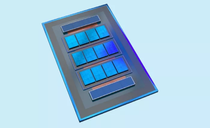
Figure 1. A rendering shows multiple chiplets connected with a combination of 2D and 3D advanced packaging techniques to create a complex system in a package.
The new technology components include:
- RibbonFET – the latest advancement in transistor architecture.
- PowerVia – the latest advancement in power delivery technology.
- Foveros Direct 3D – hybrid bonding to enable high-density direct stacking of active chips.
- Embedded Multi-die Interconnect bridge (EMIB) 3.5D – EMIB 2.5D technology combined with Foveros Direct 3D.
- Intel Foundry FCBGA 2D+ – high performance, multi-die, cost-effective, high pin-count packaging.
To read the full article, click here
Related Chiplet
- 12nm EURYTION RFK1 - UCIe SP based Ka-Ku Band Chiplet Transceiver
- Interconnect Chiplet
- Bridglets
- Automotive AI Accelerator
- Direct Chiplet Interface
Related Technical Papers
- High-performance, power-efficient three-dimensional system-in-package designs with universal chiplet interconnect express
- Intel and Cadence Collaboration on UCIe: Demonstration of Simulation Interoperability
- High-Bandwidth Chiplet Interconnects for Advanced Packaging Technologies in AI/ML Applications: Challenges and Solutions
- Defect Analysis and Built-In-Self-Test for Chiplet Interconnects in Fan-out Wafer-Level Packaging
Latest Technical Papers
- Die-Level Transformation of 2D Shuttle Chips into 3D-IC for Advanced Rapid Prototyping using Meta Bonding
- STAMP-2.5D: Structural and Thermal Aware Methodology for Placement in 2.5D Integration
- MCMComm: Hardware-Software Co-Optimization for End-to-End Communication in Multi-Chip-Modules
- FoldedHexaTorus: An Inter-Chiplet Interconnect Topology for Chiplet-based Systems using Organic and Glass Substrates
- ChipletQuake: On-die Digital Impedance Sensing for Chiplet and Interposer Verification