ATPlace2.5D: Analytical Thermal-Aware Chiplet Placement Framework for Large-Scale 2.5D-IC
ABSTRACT
The surge in consumer electronics is catalyzing the evolution of 2.5D integrated circuits (2.5D-IC). As these systems expand in scale and integrate more chiplets, the significance of chiplet design tools, particularly automatic chiplet placement, is increasingly apparent. Yet, previous studies did not sufficiently consider the distinctive features of chiplets, encountering challenges related to low quality of wirelength and poor scalability. Moreover, the pronounced high temperatures in 2.5D-ICs have not been thoroughly addressed, indicating a lack of thermal-aware design exploration. In response, this paper presents ATPlace2.5D, an analytical thermal-aware chiplet placement framework for large-scale 2.5D-ICs. It can deliver solutions that balance wirelength and temperature, residing on the optimal Pareto frontier, in collaboration with an innovative, physics based compact thermal model. Experimental results show that ATPlace2.5D can handle more than 60 chiplets in minutes, and outperforms TAP-2.5D in both maximum temperature and total wirelength by 5% and 42% in thermal-aware placement, with a 23× acceleration. This advancement holds promise for promoting the maturity and widespread application of 2.5D-ICs.
1. INTRODUCTION
Recent years have witnessed an increasing demand for cost-effective and scalable chips in various markets, such as processors, automotive electronics, and AI [1, 2]. Yet, as the development pace of advanced technology nodes slows down, the cost of designing Systems on Chip (SoC) has been on an upward trend. Against this backdrop, 2.5D integration is being increasingly recognized and explored as a means to develop cost-efficient and large-scale chip systems. 2.5D integration, as shown in Fig. 1, involves the assembly of multiple integrated circuits (ICs) that contain a well-defined subset of functionality (a.k.a. chiplets) on a single interposer, which serves as a bridge facilitating high-speed and high-bandwidth communications. It offers several advantages compared to traditional SoC [3]. Firstly, it facilitates reduced costs across the design and manufacturing stages and higher yield. Secondly, 2.5D-IC enables the seamless integration of heterogeneous technologies and nodes within a single package, i.e., System in Package (SiP). Lastly, it supports the re-using of pre-manufactured chiplets, paving the way for more sustainable and complex systems.
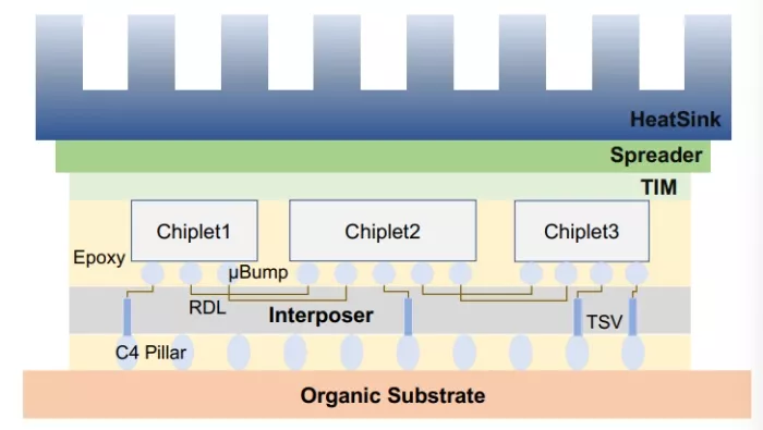
Figure 1: Illustration of the 2.5D-IC structure, fabricated with a passive interposer on an organic substrate.
To develop versatile and large-scale 2.5D-IC systems efficiently, leveraging composable chiplets (e.g., XPUs, memory, and analog modules), dedicated design automation tools are indispensable [11, 12]. Among them, we focus on the critical issue that how to arrange the placement of the chiplets to achieve optimal performance [13, 14]. Previous researches can be categorized into three types: simulated annealing (SA)-based [4–6, 15, 16], enumeration-based [7, 8, 17], and reinforcement-learning (RL)-based [9, 10]. The first type represents the layout in various manners, including vanilla layout [5], occupation chiplet matrix [6], and hierarchical B*-tree [4]. It can tackle multiple performance metrics beyond the wirelength, but often consumes significant runtime and comes to solutions of low quality. In contrast, the enumeration-based method can obtain better solutions for the placement of a few dies (typically less than a dozen), utilizing certain pruning (branch-and-bound (B&B)) and parallelization techniques [7, 17, 18]. For the last type, RL agents place chiplets one by one according to the reward function.
However, as summarized in Table 1, we recognize that these methods demonstrate poor scalability when dealing with large-scale 2.5DICs. They usually account for fewer than a dozen chiplets, whereas the scale of future 2.5D-IC systems is growing quickly beyond dozens of chiplets [19–21]. Additionally, prior efforts also suffer from low efficiency. Our study reveals that methods based on SA, enumeration, and RL all necessitate several hours to process systems comprising ten or more chiplets. This is highly time-consuming, particularly for tasks requiring iterative optimization of placement such as early-stage chiplet design space exploration [22, 23].
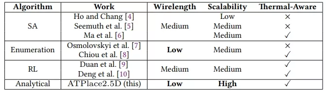
Table 1: Comparison of different chiplet placement research.
What’s worse, prior research often focuses on just reducing the area and total wirelength, which will result in compact placement results and bring about high power density, making the large-scale systems prone to thermal failure [24]. To this end, several recent research studies about thermal-aware placement for 2.5-D ICs. Coskun et al. [15] incorporate temperature constraints during SA, while TAP2.5D [6] proposes to add a term related to the worst-case temperatures in the SA cost function. SP-CP[8] introduces a post-placement procedure after the B&B search to reduce the operating temperatures by refinement. However, they often conduct thermal simulations based on numerical methods [25, 26] during the iterative optimization, which significantly augments the overall runtime. Furthermore, they typically treat temperature as a constraint, handled by controlling either the maximum temperature or minimum distance between chiplets [6, 8], lacking exploration in thermal design space, which is significant for future large-scale 2.5D-IC systems.
In this work, we aim to address these deficiencies and set up an analytical thermal-aware placement framework for 2.5D-IC. To polish up the long runtime and poor scalability, we adopt an orientationaware analytical placement algorithm [27]. In pursuit of accurate and efficient thermal evaluation, we develop a physics-based analytical compact thermal model and integrate it to optimize the overall temperature profile. Key contributions are summarized as follows:
- We propose an analytical chiplet placement framework named ATPlace2.5D, able to optimize the total wirelength and temperature simultaneously.
- We propose a new physics-based analytical compact thermal model for fast thermal simulation and optimization. It achieves a mean absolute error of ∼ 1.2 ◦C and a speedup of 2575× during thermal evaluation compared to HotSpot.
- We propose a non-linear formulation that simultaneously optimizes wirelength and temperature as an objective for both positions and orientations of chiplets.
- In a benchmark suite with a maximum case of more than 60 chiplets, ATPlace2.5D yields solutions that surpass TAP2.5D in both maximum temperature and total wirelength by 5% and 42% in thermal-aware placement, with a 23× acceleration.
The rest of the paper is organized as follows. Section 2 describes the background and preliminary; Section 3 explains the framework; Section 4 demonstrates the results; Section 5 concludes the paper.
To read the full article, click here
Related Chiplet
- Bridglets
- Automotive AI Accelerator
- Direct Chiplet Interface
- HBM3e Advanced-packaging chiplet for all workloads
- UCIe AP based 8-bit 170-Gsps Chiplet Transceiver
Related Technical Papers
- Gemini: Mapping and Architecture Co-exploration for Large-scale DNN Chiplet Accelerators
- RapidChiplet: A Toolchain for Rapid Design Space Exploration of Chiplet Architectures
- Chiplet Cloud: Building AI Supercomputers for Serving Large Generative Language Models
- A Heterogeneous Chiplet Architecture for Accelerating End-to-End Transformer Models
Latest Technical Papers
- STAMP-2.5D: Structural and Thermal Aware Methodology for Placement in 2.5D Integration
- MCMComm: Hardware-Software Co-Optimization for End-to-End Communication in Multi-Chip-Modules
- FoldedHexaTorus: An Inter-Chiplet Interconnect Topology for Chiplet-based Systems using Organic and Glass Substrates
- ChipletQuake: On-die Digital Impedance Sensing for Chiplet and Interposer Verification
- ATPlace2.5D: Analytical Thermal-Aware Chiplet Placement Framework for Large-Scale 2.5D-IC