Resonac Launches 27-Member "JOINT3" Consortium to Develop Next-Generation Semiconductor Packaging
Industry-leaders will create hub for R&D with prototype production line for 515 x 510mm panel-level organic interposers
September 03, 2025 -- Resonac Corporation (President and CEO: Hidehito Takahashi, hereinafter “Resonac”) today announced the establishment of "JOINT3," a co-creation evaluation framework formed by a consortium comprising Resonac and 26 other companies from Japan, the United States, Singapore, etc. These companies, all significant global leaders in the semiconductor supply chain, will jointly develop materials, equipment, and design tools optimized for panel-level organic interposers—semiconductor packaging technology that utilizes organic materials to create a bridge between different components on a circuit board—using a prototype production line for the manufacture of 515 x 510mm panel-level organic interposers.
Resonac will establish an "Advanced Panel Level Interposer Center (APLIC)" as the main hub for this initiative within its Shimodate Plant (Minami-yuki) in Yuki City, in Japan’s Ibaraki Prefecture. APLIC will house the prototype production line, which is scheduled to commence operations in 2026.
Here, the Consortium will accelerate development efforts by delivering verification results that closely mirror real-world structures.
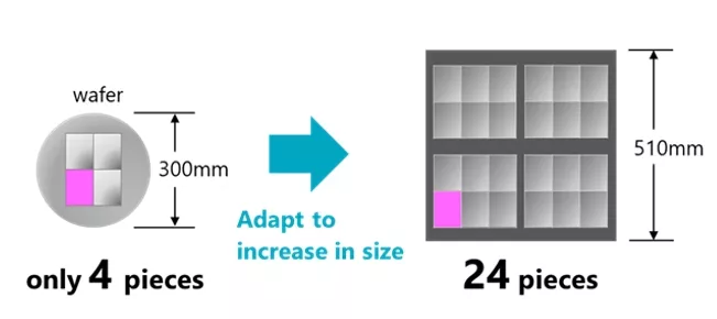
In recent years, packaging for back-end processes has emerged as a key technology in the field of next-generation semiconductors. This includes 2.xD packages, whereby multiple semiconductor chips are arranged in parallel and connected via interposers, demand for which is expected to grow in line with the need for increased data communication capacity and speed. As semiconductor performance improves, interposers are becoming larger, and there is a shift from silicon interposers to organic interposers made from organic materials.
Conventional manufacturing methods involve cutting rectangular pieces from circular wafers. However, as interposers increase in size, the number of them that can be obtained from a single wafer decreases, posing a significant challenge. To address this issue, a manufacturing process that transitions from circular wafer shapes to square panel shapes is gaining attention, as it allows for an increased number of interposers to be produced from a given area of wafer.
As leader of the JOINT3 consortium, Resonac will propose R&D priorities, managing the operation of the prototype production line and driving the overall progress of the initiative. Through co-creation with participating companies, Resonac will also promote the development of materials optimized for panel-level organic interposers.
Hidehito Takahashi, President and CEO of Resonac Holdings Corporation stated "JOINT3 brings together world-class companies from a variety of fields. Combining the complementary strengths and expertise of each company allows us to collectively address challenges in areas that were previously unreachable. This endeavor goes beyond mere technological development and will lead to solutions that address societal challenges. We are excited by the potential that this initiative offers."
Sumie Segawa, Vice President & General Manager, Division Officer, Corporate Innovation Division of Tokyo Electron Ltd., a participating company, commented, "Advanced packaging for AI semiconductors depends on miniaturization for high speed signaling and lower power, together with scaling for greater capacity. By combining JOINT3’s interposer technology with Japan’s superior materials and processing expertise, we will enable high quality, reliable manufacturing and jointly pursue further advances in AI semiconductors."
William F. Mackenzie, Group Managing Executive Officer, Ushio Inc., another participating company, remarked, " Advanced packaging is entering a new era, demanding innovation and collaboration across the ecosystem. As a core enabler, lithography is key to meeting these challenges. Through our Digital Lithography Technology and partnership in the JOINT3 consortium, Ushio is working with industry leaders to deliver the precision and performance the future demands."
JOINT3 Logo(Participating company logos)
Resonac will leverage the knowledge gained from the semiconductor packaging technology development consortia "JOINT" and "JOINT2," which transcend the boundaries of semiconductor equipment and materials manufacturers, as well as that sourced from "US-JOINT," which is being developed in Silicon Valley in the United States. By doing so, Resonac aim to contribute to technological innovation in next-generation semiconductor packaging.
Overview of JOINT3
| Name | JOINT3 (JOINT:Jisso Open Innovation Network of Tops) |
|---|---|
| Objectives | Accelerate the development of materials, equipment, and design tools optimized for panel-level organic interposers through co-creation with participating companies |
| Participating Companies (listed in alphabetical order) |
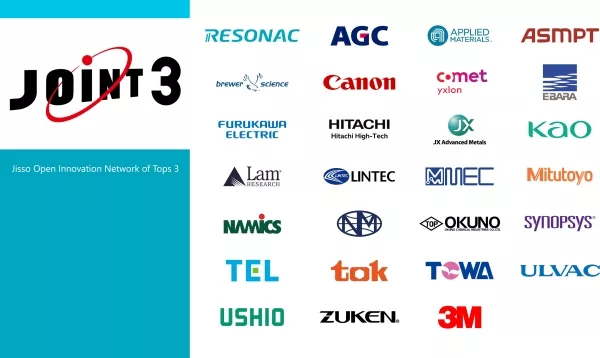
27 companies (as of September 3, 2025) Resonac Corporation, AGC Inc., Applied Materials, Inc., ASMPT Singapore Pte. Ltd., Brewer Science, Inc., Canon Inc., Comet Yxlon GmbH, EBARA Corporation, Furukawa Electric Co., Ltd., Hitachi High-Tech Corporation, JX Advanced Metals Corporation, Kao Corporation, Lam Research Salzburg GmbH, LINTEC Corporation, MEC COMPANY LTD., Mitutoyo Corporation, NAMICS Corporation, Nikko-Materials Co., Ltd., OKUNO CHEMICAL INDUSTRIES CO., LTD., Synopsys, Inc., Tokyo Electron Ltd., Tokyo Ohka Kogyo Co., Ltd., TOWA Corporation, ULVAC, Inc., Ushio Inc., ZUKEN Inc., 3M Company |
| Location | -Advanced Panel Level Interposer Center “APLIC” (Yuki City, Ibaraki Prefecture, Japan (within the Resonac Shimodate Plant) -Packaging Solution Center (Kawasaki City, Kanagawa Prefecture, Japan) |
| Activities | -Developing materials, equipment, and design tools for organic interposers using a panel-level (515 x 510 mm) prototype production line -Promoting development through co-creation by having material and equipment manufacturers produce common prototypes -Utilizing JOINT3 as a “training ground” for technology and equipment manufacturers to further enhance technologies related to panel-level organic interposers |
Supplementary Materials: Overview of Companies Participating in JOINT3
Company Name: AGC Inc.
Position in Industry: AGC provides products in the semiconductor-related field, ranging from inorganic materials such as glass to organic materials and composite products that combine both. With over 110 years of history since its founding, the company leverages its expertise in material design and processing technologies to contribute to the development of materials for next-generation semiconductor packaging.
Quote: AGC will leverage its diverse material technologies in both inorganic and organic fields to provide innovative and high-quality glass carriers and interposer glass products to the JOINT3 Consortium. By closely collaborating with participating companies, we aim to contribute to the establishment and the de facto standardization of panel-level process technology, which is expected to become the foundation for next-generation semiconductor packaging technologies.
Company Name: Applied Materials, Inc.
Position in Industry: Applied Materials, Inc. (Nasdaq: AMAT) is the leader in materials engineering solutions that are at the foundation of virtually every new semiconductor and advanced display in the world. The technology we create is essential to advancing AI and accelerating the commercialization of next-generation chips. At Applied, we push the boundaries of science and engineering to deliver material innovation that changes the world. Learn more at https://www.appliedmaterials.com.
Quote: Applied Materials looks forward to bringing our expertise in materials engineering to the JOINT3 initiative and contributing to the progress of advanced packaging technologies. This consortium is a valuable opportunity to collaborate with industry partners to expand the advanced packaging ecosystem and enable new architectures using panel-level technologies, and we are excited to help accelerate these innovations.
Company Name: ASMPT Singapore Pte. Ltd.
Position in Industry: Headquartered in Singapore, ASMPT is a leading global supplier of hardware and software solutions for the manufacture of semiconductors and electronics across semiconductor assembly & packaging, and SMT industries. It is an advanced packaging leader with the largest installed base of TCB tools in the world.
Quote: Participation in JOINT3 represents a natural extension of our leadership in advanced packaging technologies. Bringing our market-leading thermo-compression bonding (TCB) expertise to enable panel-level manufacturing capabilities (with more than 500 TCB systems deployed in mass production worldwide), we have established the industry standard for precision heterogeneous integration across 2D, 2.5D, and 3D packaging formats. Our proven track record spanning chip-to-substrate, chip-to-wafer, and HBM applications, combined with our unique position as the consortium's sole back-end assembly specialist, enables us to serve as JOINT3’s critical bridge between panel-level packaging innovation and manufacturing reality.
Company Name: Brewer Science, Inc.
Position in Industry: Brewer Science is a global leader in developing and manufacturing next-generation materials and processes that foster the technology needed for tomorrow. Since 1981, we’ve expanded our technology portfolio within advanced lithography, advanced packaging, smart devices, and printed electronics to enable cutting-edge microdevices.
Quote: At Brewer Science, our participation in the JOINT3 Consortium reflects our continued commitment to driving innovation in the semiconductor industry. Leveraging our advanced materials expertise, particularly in high-performance polymer solutions, we collaborate with industry leaders to pioneer technologies that enable smarter, more sustainable solutions. Through this consortium, we aim to accelerate the development of next-generation semiconductor packaging, supporting a connected, intelligent, and environmentally responsible future.
Company Name: Canon Inc.
Position in Industry: Canon’s Industrial Group offers a broad portfolio of semiconductor manufacturing equipment. Its FPA-5520iV lithography system plays a key role in advanced packaging, enabling high-precision patterning for cutting-edge semiconductor devices.
Quote: As AI processors continue to increase in computing power, package sizes are expanding. With this trend, the inefficiency of wafer level packaging has become a challenge, and panel level packaging is being proposed as a new approach.
Canon is committed to driving innovation in panel level packaging by leveraging our technologies and expertise in wafer level packaging with JOINT3 members. Through this innovation, Canon aims to enhance both the performance and cost-efficiency of AI processors.
Company Name: Comet Yxlon GmbH
Position in Industry: Powered by decades of x-ray and CT leadership, Comet Yxlon delivers high-end industrial inspection solutions, increasingly focused on the semiconductor industry. Its x-ray systems make the invisible visible through cutting-edge imaging, AI enhanced analytics, and intuitive interfaces, enabling manufacturers to innovate with confidence, accelerate time to market, and dramatically improve yield and efficiency. See Better. Faster. More.
Quote: With its recently launched CA20 x-ray system, Comet Yxlon sets a new benchmark in non-destructive 3D inspection for advanced semiconductor packaging. Developed specifically for the industry, it delivers sub-micron resolution via cutting-edge computed laminography, revealing defects in seconds that once took weeks to detect. From chiplets to HBM stacks, CA20 drives the “More-than-Moore” future with unmatched clarity and speed. While early use focused on micro-bumps, its application range is far broader, opening doors to technologies not yet imagined. These insights, impossible before, will give our partners a decisive edge in developing tomorrow’s semiconductor innovations.
Company Name: EBARA Corporation
Position in Industry: EBARA Corporation has a broad product portfolio in the semiconductor field, consisting of two businesses: equipment and components. In the equipment business, we provide CMP equipment, plating equipment, and bevel grinding equipment, contributing to the development of the semiconductor industry.
Quote: We expect that the importance of panel-level packaging will increase in the future due to the increase in package size by improvements in the functionality and performance of AI and HPC semiconductors. By participating in the JOINT3 Consortium, we aim to improve the technical capabilities of panel-level CMP equipment through collaboration with participating companies, while utilizing our technical capabilities and experience cultivated at the wafer level.
Company Name: Furukawa Electric Co., Ltd.
Position in Industry: Furukawa Electric supports the electronics industry with a diverse range of products, including optical semiconductor lasers, electrolytic copper foil, and heat sinks. Its adhesive tapes and bonding films for semiconductor back-end processes are highly regarded for their functionality and quality, contributing to the industry's advancement.
Quote: This year marks the 40th anniversary of Furukawa Electric’s commercialization of adhesive tape products for semiconductor back-end processes. Leveraging our accumulated technological expertise and proposal capabilities, we have refined our adhesive technologies by incorporating customer feedback. We are honored to have the opportunity to participate in the JOINT3 consortium. Through co-creation with fellow participating companies, we aim to further enhance our technological capabilities, take on the challenge of innovating next-generation semiconductor packaging technologies, and contribute to the development of the semiconductor industry.
Company Name: Hitachi High-Tech Corporation
Position in Industry: Hitachi High-Tech’s products span the etching, measurement, inspection systems, and electron microscopes in semiconductor manufacturing processes, including global top-selling CD-SEM. We are contributing to technological innovation in advanced semiconductor devices and manufacturing process.
Quote: We are honored to participate in the JOINT3 Consortium, which is expected to further accelerate the growth of the semiconductor industry. Hitachi High-Tech offers a wide range of solutions, from semiconductor manufacturing equipment for etching, measurement and inspection, to electron microscopes which are essential for R&D. By leveraging our broad expertise and collaborating closely with other member companies, we are committed to contributing to the advancement of next-generation semiconductor packaging technologies.
Company Name: JX Advanced Metals Corporation
Position in Industry: JX Advanced Metals is a global leader in advanced materials, delivering high-performance solutions derived from copper and rare metals. Our flagship products include sputtering targets for semiconductors and rolled copper foils, and we proudly hold the world’s top market share across a wide range of products.
Quote: We are truly honored to have the opportunity to contribute to the advancement of the cutting-edge semiconductor industry through our participation in JOINT3. Our company possesses a wide array of development-stage materials with potential applications in advanced packaging technologies. Leveraging this collaboration, we will further promote initiatives aimed at the development and practical implementation of new materials through co-creation with fellow participating companies, while striving to generate sustainable value.
Company Name: Kao Corporation
Position in Industry: Kao is a global leader of Fine Cleaning. Building on our “Interfacial Science Technology”, we provide high performance and eco-friendly chemicals for the semiconductor industry including Deflux, Etching, Polishing, Stripping agents, and Insulating/Conductive materials.
Quote: For more than 140 years since Kao was founded in 1884, we have enhanced “Interfacial Science Technology” to provide cleaning solutions across a wide range of fields - from consumer products to industrial applications. In particular, in the field of Fine Cleaning for Semiconductor, we are advancing the development of technologies and products with the aim of “creating Kirei surface for forefront semiconductors toward future”. At JOINT3, we will take on the challenge of further advancing cleaning solutions based on our technologies and expertise we have cultivated, in order to contribute to the growth of the future semiconductor industry.
Company Name: Lam Research Salzburg GmbH
Position in Industry: Lam Research is a global supplier of innovative wafer fabrication equipment and services to the semiconductor industry. Lam’s equipment and services allow customers to build smaller and better performing devices. We combine superior systems engineering, technology leadership, and a strong values-based culture, with an unwavering commitment to our customers.
Quote: Lam Research’s leadership position in critical etch and deposition segment of advanced packaging solutions enables heterogeneously integrated products for high bandwidth memory (HBM), AI CPUs, and GPUs. Our industry-leading tools and technologies deliver the precision, production yields, and cost efficiencies needed to scale beyond Moore’s Law through new approaches to 3D stacking and chiplet integration. Now, Joining the Joint3 consortium positions us to help drive advanced substrate technology into the new era, powered by our cutting-edge panel process capabilities.
Company Name: LINTEC Corporation
Position in Industry: Since launching our semiconductor-related business in 1986 with the development of UV-curable dicing tape, LINTEC has continuously developed and manufactured high-performance tapes that leverage its unique adhesive technologies and related equipment designed to maximize tape performance.
Quote: The name “LINTEC” derives from a combination of “linkage” and “technology,” reflecting the company’s mission of integrating technologies to generate synergistic value through innovation. By combining its core adhesive technology with proprietary equipment technologies, LINTEC has broken through conventional semiconductor manufacturing processes to realize its unique ideas. Through its participation in the JOINT3 project and collaboration with fellow member companies, LINTEC is committed to creating its own unique technique and contributing to the advanced packaging technologies.
Company Name: MEC COMPANY LTD.
Position in Industry: MEC was founded in 1969. Since then, we have established various metal surface treatment technologies, including chemical etching and functionalization solutions, those create additional value at interfaces. Today, our chemicals are widely adopted in semiconductor substrate manufacturing and are acknowledged as an indispensable process.
Quote: Through the JOINT 3 consortium, MEC will be committed to driving breakthrough innovations and technological advancement for the semiconductor industry. We will effectively collaborate with industry-leading partners to create new value, applying our unique metal surface processing technologies and expertise cultivated through years of experience in the semiconductor package substrate field. We hope our active engagement in this ambitious consortium will contribute to the technology evolution at the forefront of next-generation semiconductor packaging and be enabling us to play a significant role in the digital transformation of society and the development of a more sustainable future for all.
Company Name: Mitutoyo Corporation
Position in Industry: With extensive expertise in high-precision measurement of fine structures and multilayer interconnects for advanced packaging, we work closely with semiconductor-related companies in Japan and abroad as a trusted metrology partner supporting reliability evaluation and quality assurance in back-end processes.
Quote: Through this consortium, we are honored to provide optimal solutions to the increasingly diverse and high-precision measurement challenges required for advanced packaging. At the same time, we find it highly meaningful to engage in co-creating next-generation metrology technologies with participating companies, to lead the industry. We will continue to pursue technological innovation and remain dedicated to maximizing customer value.
Company Name: NAMICS Corporation
Position in Industry: NAMICS has over 30 years of experience in the semiconductor materials field and is a leading company in the development and manufacturing of liquid semiconductor encapsulants. Through creative and innovative technology, we provide essential materials for next-generation semiconductor packaging.
Quote: Through our participation in the JOINT3 consortium, we aim to accelerate technological innovation in the semiconductor packaging industry. By leveraging our expertise in the development of liquid semiconductor encapsulants and collaborating with participating companies, we will create new value and contribute to the realization of a sustainable society. We hope that the activities of this consortium will be an important step in supporting the evolution of next-generation packaging technology.
Company Name: Nikko-Materials Co.,Ltd.
Position in Industry: Nikko-Materials has been a leading company in vacuum lamination technology in the electronics industry for over 20 years, manufacturing and selling equipment and providing solutions related to the lamination of various film materials.
Quote: We will contribute to the creation of next-generation semiconductor packaging technology in the JOINT3 consortium by leveraging the vacuum lamination technology we have cultivated to date. As a manufacturer of vacuum lamination equipment, we hope to play a part in advancing technology in this field by leveraging our expertise in bonding film materials under vacuum without voids or wrinkles, in cooperation with participating companies.
Company Name: OKUNO CHEMICAL INDUSTRIES CO., LTD.
Position in Industry: Okuno Chemical Industries celebrates its 120th anniversary and is a leading company with strong research and development capabilities in the field of surface treatment and plating chemicals. It has particular expertise in chemicals and equipment for semiconductor package substrates.
Quote: About one-third of all employees at Okuno Chemical Industries are researchers, primarily engaged in process development for surface treatment chemicals and plating equipment, especially in the semiconductor field. We provide plating chemicals for applications such as RDL (Re-Distribution Layer), copper/nickel bumps, and mega-pillar formation. Through these products, we support technological innovation in the next-generation semiconductor packaging industry.
Company Name: Synopsys, Inc.
Position in Industry: Synopsys, Inc. (Nasdaq: SNPS) is the leader in engineering solutions from silicon to systems, enabling customers to rapidly innovate AI-powered products. We deliver industry-leading silicon design, IP, simulation and analysis solutions, and design services. We partner closely with our customers across a wide range of industries to maximize their R&D capability and productivity, powering innovation today that ignites the ingenuity of tomorrow. Learn more at www.synopsys.com.
Quote: New breakthroughs in chip packaging are critical to achieve increasing levels of performance, energy efficiency and manufacturability of complex AI silicon, and panel-level interposer packaging holds promise as a cost-effective and adaptable platform,” said Steve Pytel, vice president of product management at Synopsys. “We’re proud to contribute our expertise and industry-leading design solutions to the new Joint3 consortium. Access to Synopsys’ multiphysics simulation, design validation and virtual prototyping solutions will enable cross disciplinary collaboration and help consortium partners rigorously validate their concepts and accelerate the delivery of market-ready panel-level interposer technologies.
Company Name: Tokyo Electron Limited (TEL)
Position in Industry: TEL holds one of the largest shares in the global semiconductor production equipment market. The company provides a wide variety of semiconductor production equipment with superior processing and production capabilities. TEL’s offerings include deposition, coating/developing, etching, cleaning, probing, and bonding/debonding systems, as well as reliable technical support services.
Quote: We are participating in JOINT3 to contribute to the ever-accelerating development of AI semiconductors. Among the development objectives of JOINT3, we are particularly interested in enhancing interposers with higher-density interconnects and larger dies because they are critical to developing future AI semiconductors. Our high-precision technologies, developed for demanding front-end semiconductor processes, will now be integrated with Japan’s world-leading materials engineering technologies. We are confident that these collaborative efforts will result in higher quality and yields, fueling the future evolution of semiconductors.
Company Name: Tokyo Ohka Kogyo Co., Ltd.
Position in Industry: Tokyo Ohka Kogyo is a leading company in the photoresist industry. Based on its technological strength in developing Japan’s first semiconductor photoresist, the company continues to lead the field and actively expands into next-generation semiconductor packaging materials.
Quote: In the rapidly growing semiconductor packaging field, we are taking on the challenge of new Panel Level Packaging (PLP) technologies through the JOINT3 consortium. Driven by intellectual curiosity and a spirit of innovation, we aim to accelerate technological advancement alongside our partners by leveraging our high-performance, high-purity photoresists. Through chemistry, we strive to meet societal expectations and contribute to a sustainable future.
Company Name: TOWA Corporation
Position in Industry: TOWA is a leading company with the world’s top market share in the semiconductor molding equipment sector. We possess unique strengths in advanced packaging technologies and provide solutions that support the evolution of the industry.
Quote: As the advanced semiconductor industry continues to evolve at a remarkable pace, there are high expectations worldwide for further developing PLP processes. Through the collaboration of material and equipment manufacturers facilitated by JOINT3, we are extremely hopeful that sharing information and technical expertise between companies will create an environment conducive to innovation and thus help accelerating the development of complex processes.
TOWA will participate with a primary focus on molding, contributing to the development of PLP processes within this consortium, the growth of participating companies, and the further advancement of the semiconductor industry.
Company Name: ULVAC, Inc.
Position in Industry: ULVAC is an equipment manufacturer that develops and supplies deposition and plasma processing equipment based on its core vacuum technology. In the next-generation semiconductor packaging field, we provide industry-leading process equipment featuring high-precision deposition and plasma processing technologies.
Quote: We are introducing the sputtering equipment for seed layer and leveraging our expertise in process technology to contribute to the advancement of next-generation semiconductor packaging technology. Through collaboration with participating companies, we will share challenges in packaging technology and co-create its future vision. We are confident that the activities of this consortium will be an important step towards supporting the advancement of next-generation semiconductor packaging technology.
Company Name: Ushio Inc.
Position in Industry: Ushio offers a complete lithography portfolio for advanced package substrates, including steppers, DI exposure systems, and cutting-edge digital lithography. Through our strategic partnership with Applied Materials, Inc., we deliver innovative solutions that meet evolving substrate requirements and enable the next generation of advanced packaging technologies.
Quote: As semiconductor package substrates for AI chips require not only miniaturization but also larger sizes and increased complexity to support diverse packaging formats, various technical challenges have emerged. Ushio is collaborating with ecosystem partners to address these lithography challenges by utilizing our digital lithography technology. Through the JOINT3 Consortium, we address various challenges in the manufacturing processes of advanced package substrates from the perspective of lithography technology, contributing to the establishment of mass production technologies.
Company Name: ZUKEN Inc.
Position in Industry: Zuken’s EDA solutions are trusted by many of the world’s leading companies in industries such as Electronic Components, Automotive, and Industrial Machinery—sectors that demand advanced electrical and electronic system design and verification. Through advanced services and robust technical solutions, Zuken supports the development of high-quality products.
Quote: Through our participation in JOINT3, Zuken will contribute to the design, manufacturing, and validation of next-generation semiconductor packaging using panel-level organic interposers, leveraging our EDA tools and design/verification technologies. We are also exploring early-stage verification approaches that take into account the physical characteristics and properties of various materials during the design phase. By cooperating and collaborating with other JOINT3 members, we aim to be a trusted and reliable partner in the next-generation ecosystem and supply chain.
Company Name: 3M Company
Position in Industry: For over 25 years, 3M has delivered innovative solutions to the semiconductor industry, taking on our customers’ toughest challenges from chip fabrication to advanced packaging. Powered by global capabilities and materials science innovation, we enhance product performance, boost process efficiency and yield, and reduce total cost of ownership, meeting advanced roadmap requirements.
Quote: 3M, a global leader in materials science and innovation, is excited to partner with Resonac and other semiconductor industry leaders through the JOINT3 co-creative evaluation platform to advance Panel Level Packaging (PLP). As crucial drivers of device performance and systems innovation, advanced packaging technologies like PLP are essential for fabricating next-generation AI and high-performance chips. This collaboration aims to accelerate integrated total solution readiness, addressing stringent performance and cost requirements. We are eager to contribute our key technology platforms and solutions, providing decades of expertise to help shape the future of advanced packaging and drive progress in semiconductor manufacturing and roadmap advancement.
Related Chiplet
- DPIQ Tx PICs
- IMDD Tx PICs
- Near-Packaged Optics (NPO) Chiplet Solution
- High Performance Droplet
- Interconnect Chiplet
Related News
- Resonac and PulseForge Unite to Advance Photonic Debonding for Next-Gen Semiconductor Packaging
- UCIe Consortium Releases 2.0 Specification Supporting Manageability System Architecture and 3D Packaging
- Global Semiconductor Packaging Material Market Outlook Shows Return to Growth Starting in 2024
- KLA Unveils Comprehensive IC Substrate Portfolio for a New Era of Advanced Semiconductor Packaging
Latest News
- IC-Link by imec joins TSMC 3DFabric® Alliance to accelerate advanced packaging and 3D IC innovation
- EXTOLL announces Availability of Industry's first 16G UCIe PHY IP in GlobalFoundries 22FDX/22FDX+ Ready for Customer Integration
- NHanced Semiconductors & Florida State University to Present on Hybrid Bonding Reliability at the 2026 Electronic Components & Technology Conference in Orlando
- Wooptix Targets AI Packaging Bottleneck with Astronomy Tech
- Kenyi Technologies to collaborate with ADTechnology to co-develop a Server Processor targeting Edge AI and Telco use cases