Berkeley Lab and Open Compute Project Collaborate to Advance Chiplet Technology for HPC
October 16, 2024 -- Progress used to be made by leaps and bounds in the never-ending race to improve the performance of the latest generation of supercomputers. But now, scientists are hitting a wall.
High-performance computing (HPC) systems—which help researchers push the boundaries of what is possible in science and innovation—used to grow 1,000 times faster and more powerful every 11 years. That performance improvement rate has since been “dropping precipitously,” down to a fivefold gain—or less—every decade, said John Shalf, who leads the Computer Science Department within the Applied Math and Computing Sciences Division (AMCR) at Lawrence Berkeley National Laboratory (Berkeley Lab).
“The future of HPC looks really bleak if we continue doing things the way that we're currently doing them. Our current approach has served HPC well for decades, but has been running out of steam this past decade,” said Shalf. “I see chiplets as an opportunity to restore our historical growth rate of energy efficiency and performance.” Chiplets are a novel form of advanced silicon packaging—a highly modular design approach—that enables innovative specializations to be incorporated into future HPC chips. This could potentially help to regain some of the momentum from the halcyon days of HPC innovation.
With the rise of chiplets, Shalf saw an opportunity for Berkeley Lab and the U.S. Department of Energy (DOE) to collaborate with hyperscalers – large cloud services providers like Amazon, Google, Microsoft, and others – via forums such as the Open Compute Project to leverage the larger industry trends to benefit HPC. While it is still in the early stages, this collaboration is already producing tangible results, as evidenced by the Open Chiplet Economy Experience Center, launched at Berkeley Lab earlier this year. The center holds technical demonstrations on the latest advancements in the emerging chiplet market.
Chiplets Demystified and Deconstructed
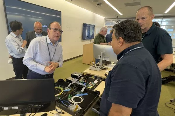
Open Compute Project Chief Innovation Officer Cliff Grossner (left) demonstrates technology at the launch of Berkeley Lab's Open Chiplet Economy Experience Center in June 2024. (Photo by Hui Zhang, Berkeley Lab)
“The challenge with traditional monolithic dies [or integrated circuits fabricated on a single piece of silicon] is that manufacturers are starting to hit the limits of how big they can make them while still trying to pack the same punch in terms of performance. That means that they’re not only becoming more and more expensive, but the likelihood of a fatal defect that renders the chip unusable increases significantly,” said Shalf.
So what exactly are chiplets, and why are they better? Instead of building all the necessary circuitry on a single monolithic die, chiplets break down a large chip into smaller functional blocks. This allows for a mix-and-match approach in hardware design and provides opportunities to reuse components across technology generations and to include specialized components for specific workloads.
Mainstream suppliers such as AMD, NVIDIA, and Intel already rely on chiplets for machines operating in DOE HPC centers.
“The long-term vision being pioneered by organizations such as the Open Compute Project’s Open Chiplet Economy Project (formerly Open Domain Specific Architecture) is to create an open economy where an integrator can create unique products by co-integrating chiplets from multiple suppliers by way of standardized tools automating the design and manufacturing of chiplet-based products and standard interfaces such as UCIe and BoW,” said Open Compute Project Chief Innovation Officer Cliff Grossner. This vision for the future is referred to as the “open chiplet economy.”
According to Shalf, chiplets also present a notable advantage by significantly lowering the risk of fatal defects compared to traditional monolithic integration methods. He explains that the yield curve—indicating the number of functional chips produced at the largest size possible with the latest chip manufacturing equipment—is much lower for monolithic dies than for modular packages made from smaller dies. In the worst-case scenario, up to nine out of ten chips could fail, significantly impacting technology firms’ profitability.
The chiplet approach, on the other hand, allows scientists and engineers to test each of these smaller chiplets, see which ones are tested and known to be good (“known good die”), and then assemble them into the package. In other words, it reduces the likelihood of fatal defects. Shalf points out that “AMD published a 2021 paper at the International Symposium on Computer Architecture (ISCA) that provides insight into the yield advantages and cost model of moving to chiplets.” Furthermore, this approach enables manufacturers to break through the reticle limit. You can actually have packages that are super chips that are even larger than what you could do with a monolithic die.
Another advantage of chiplets that Shalf and Grossner identify is the opportunity to insert specialization without owning the design of the entire chip. The vision is that specializations can be inserted into mainstream designs at lower cost using chiplets as the vehicle. Currently, this is being done within companies using their own library of available components, but in the near future, there are opportunities for pair-wise engagements with technology companies to collaborate with a customer to insert specializations (in the form of chiplets) into their existing products.
To Shalf, that constitutes the next step in the chiplet and HPC crossover: “Instead of repurposing hardware designed for a different market, chiplets could be tailor-made for the science space. Chiplets lower the barriers to insert some custom features for a particular customer when the rest of the chiplets in the package remain standard, for example, the insertion of workload-specific functionality to accelerate high-value HPC apps and AI.”
Work To Do: From Chiplet Standardization to Security
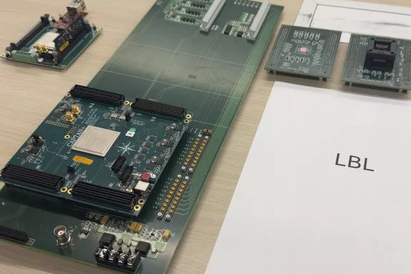
Berkeley Lab's Project 38 demonstration at the launch of the Lab's Open Chiplet Economy Experience Center. (Photo by Hui Zhang, Berkeley Lab)
While the broader adoption of chiplets shows promise for scientists and researchers—evidenced by the chiplet-based Frontier supercomputer at DOE’s Oak Ridge National Laboratory—significant challenges remain.
To effectively mix and match chiplets from multiple sources, a set of guidelines for applying open standards is essential for a family of chiplets aimed at a specific market. This is similar to the guidelines for PCIe cards or storage devices, which specify certain form factors and power envelopes to ensure compatibility for easy server integration.
“Open standards are emerging, but they aren’t settled on the die-to-die interface between the chiplets,” Shalf said. “Right now, what Intel uses internally and what AMD uses internally are different.”
“We believe there is no universal standard that will fit all use cases,” Grossner adds.
They both note that as the market emerges, we are learning that there needs to be a consensus on the chiplet package itself. Specifically, the mechanical aspects, form factors, pin-spacings, and other physical packaging choices must be agreed upon. There is some evidence that the needs of the automotive market, for instance, will be different from the needs for hyperscale computing, AI, and HPC.
Another sticking point is security. “If you’re working with third-party chiplets, you don’t want some bad actor to come in and insert some Trojan horse chiplet,” Grossner said. “So we need to have some kind of a security approach to provide a hardware-based root of trust ensuring all chiplets within the package act with integrity.”
Software interfaces need to be worked out too. “If you have diverse hardware, you need to have a common way in the software to access that hardware. This is uncharted territory for security and software, so there is a lot of research left to be done to make this safe for commercial deployment,” said Shalf.
And while vertically integrated companies, like Intel or AMD, have done so internally, third parties need to be able to collaborate for an open chiplet marketplace to truly thrive. Right now, big manufacturers such as Intel, AMD, and Arm are considering offering a path for a bespoke chiplet to be dropped into their platform as long as it conforms to their proprietary engineering design rules. “However, it isn’t interchangeable across other platforms,” Grossner said.
He notes that hyperscalers are pushing an open chiplet marketplace where the standard is such that it is portable between multiple vendors. “So I can insert my chiplet into a package with Arm, but I could also insert my chiplet into a package with AMD. We’re not there yet, but it is a big vision for the future,” Grossner adds.
‘A Totally New Supply Chain for Silicon’
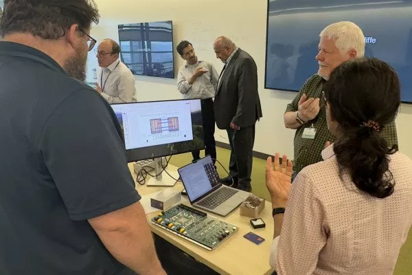
Synopsys technology demonstration at Berkeley Lab's Open Chiplet Economy Experience Center launch in June 2024. (Photo by Hui Zhang, Berkeley Lab)
Berkeley Lab and the Open Compute Project Community came up with a strategy involving the use of modular chiplets as a way to integrate HPC-relevant specializations so they could remain competitive and yet reuse elements of the design, such as the CPUs, memory controllers, and other parts. Without reusable components, engineering costs would skyrocket, so figuring out what functionality is in the broadest interest is crucial.
“Hyperscalers – which account for about half of all server-class microelectronics equipment purchases worldwide – had recognized that they needed to insert their own specializations into the hardware to get a leg up on performance and energy efficiency,” said Grossner.
"I noticed that the specialization strategies being planned by the hyperscalers for the cloud could also be leveraged by HPC to tailor our platforms for the same reasons the hyperscalers are adopting this approach," Shalf said. “So our lab became a member of the Open Compute Project, which is a collaborative community that the hyperscalers have created to solve shared problems like these.”
Initiated in 2011 “with a mission to apply the benefits of open source and open collaboration to hardware,” the Open Compute Project Foundation set out to spur innovation and support the growing demands on computing infrastructure.
“The Open Compute Project Community provides open specifications for hardware, community-developed standardizations, white papers covering best practices, and system architecture blueprints,” said Grossner.
The idea is to create an open chiplet economy where chiplets are designed by different companies for particular functions. Those chiplets are then sold on the market to a packaging house that stitches the chiplets together onto a running circuit.
“That’s a totally new supply chain for silicon,” Grossner said. “But it opens up the old silicon development process, allowing even small companies potentially to get involved, be innovative, design a chiplet, make it available – and others can buy it and use it and combine it with chiplets from other vendors to create a final package that has the performance desired at the cost curve desired.”
According to Grossner, it’s “very early days” for the open chiplet economy. Standards around modularization for chiplets are still needed. An Open Compute Project workstream led by Berkeley Lab is looking at common form factors that can be used to design chiplets for HPC and artificial intelligence.
“It’s going to be a 10-year journey before chiplets are truly interoperable across vendors and foundries,” Grossner said of the open chiplet economy effort. “But chiplets are already here and their footprint on the electronics industry continues to grow.”
About Berkeley Lab
Founded in 1931 on the belief that the biggest scientific challenges are best addressed by teams, Lawrence Berkeley National Laboratory and its scientists have been recognized with 16 Nobel Prizes. Today, Berkeley Lab researchers develop sustainable energy and environmental solutions, create useful new materials, advance the frontiers of computing, and probe the mysteries of life, matter, and the universe. Scientists from around the world rely on the Lab’s facilities for their own discovery science. Berkeley Lab is a multiprogram national laboratory, managed by the University of California for the U.S. Department of Energy’s Office of Science.
DOE’s Office of Science is the single largest supporter of basic research in the physical sciences in the United States, and is working to address some of the most pressing challenges of our time. For more information, please visit energy.gov/science.
Related Chiplet
- DPIQ Tx PICs
- IMDD Tx PICs
- Near-Packaged Optics (NPO) Chiplet Solution
- High Performance Droplet
- Interconnect Chiplet
Related News
- InPsytech showcases 3nm UCIe 3.0 technology at OCP 2025, Accelerating Innovation in Chiplet Ecosystem
- Eliyan Showcases Next-Generation Chiplet Interconnect and Memory Innovations at OCP Global Summit 2025
- Ayar Labs Unveils World's First UCIe Optical Chiplet for AI Scale-Up Architectures
- NcodiN secures €3.5 M for optical interposer tech to meet the needs of HPC and AI
Latest News
- NIST Researchers Develop Photonic Chip Packaging That Can Withstand Extreme Environments
- Rebellions Closes $400 Million Pre-IPO and Launches RebelRack™ and RebelPOD™ to Accelerate Global Expansion
- EdgeCortix Looks To Chiplets For Third-Gen Reconfigurable AI Chip
- Agileo Automation Launches Agil'EDA to Accelerate SEMI EDA Adoption for Semiconductor Equipment OEMs
- AEM and ASE Enter Strategic Partnership to Accelerate AI and HPC Test Innovation