A Guide to Building Chiplets Today While Shaping Tomorrow’s Standards

Chiplet standards may still be evolving, but here’s a guide to what you can do now to build with chiplets today.
Every major semiconductor design shift requires balancing what is possible today with what will be standard tomorrow. As systems-on-chip (SoCs) push past the boundaries of reticle limits, chiplets are an emerging technology that offers a practical path forward. Current chiplet standards provide only a partial framework for today’s multi-die architectures. However, starting designs now delivers practical benefits and allows engineers to influence the standards that will guide the industry for years.
Standards are still under construction
Chiplet standards that define how dies communicate, exchange data reliably, and integrate into larger systems are currently being developed. Despite varying development timelines, the standards are still years from maturity, as their efforts include different levels of scope and complexity. However, the common goal is to create universal standards that allow teams to integrate chiplets from multiple sources without restriction. Three initiatives stand out as the most visible efforts toward standardizing chiplet integration.
A broad coalition of semiconductor leaders backs universal Chiplet Interconnect Express (UCIe). UCIe defines a common physical and protocol layer for die-to-die connectivity and benefits from support from EDA, foundries, and IP companies. UCIe is advancing, with version 1.1 released in 2024, and is expected to reach broad, stable maturity around 2029–2030.
Advanced Interface Bus (AIB), developed by Intel and now under CHIPS Alliance, targets short-reach, low-latency links. While AIB can be considered mature for small niche applications, broader adoption of commercial multi-die packages will not be ready until 2026–2027.
Bunch of Wires (BoW), from the Open Compute Project’s ODSA group, emphasizes simplicity and efficiency for low-power, cost-sensitive applications by trading off density and speed in favor of lightweight implementation. Adoption is building but is not likely to materialize until 2027–2028.
Building designs with chiplets now
Chiplet adoption can follow a natural crawl-walk-run progression. The early stage begins with straightforward steps that improve current projects while preparing for broader use over time, as shown in Figure 1.
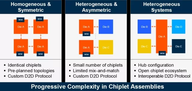
Figure 1. Progressive complexity in chiplet assemblies. (Source: Arteris, Inc.)
Practical strategies for design teams to consider include:
- Adopt IP packaging methodologies to ensure consistency and enable reuse.
- Apply partitioning strategies now to improve yield and manufacturability.
- Invest in connectivity solutions that accommodate both coherent and non-coherent compute.
For engineers who are ready to act today, a more detailed implementation is described below, as shown in Figure 2.
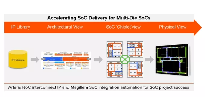
Figure 2. Arteris NoC interconnect IP and Magillem SoC integration automation for SoC project success. (Source: Arteris, Inc.)
- Establish standardized integration views by applying packaging automation with the IEEE 1685 (IP-XACT) standard, producing IP metadata, memory and register maps, and port/bus interface descriptions that can be reused across designs. This enables the assembly of IP and subsystems from multiple sources. It provides chiplets with the correct-by-construction framework necessary for seamless plug-and-play integration into larger multi-die systems.
- Inside the SoC, incorporate cache-coherent and non-coherent interconnect fabrics to provide high-bandwidth, scalable infrastructure. Non-coherent interconnects route traffic efficiently with low latency and optimized power, while cache-coherent designs ensure that CPUs, GPUs, and accelerators maintain consistency across shared memory. Together, they deliver quality-of-service features and predictable performance, enabling SoCs and chiplets to function as reliable building blocks within larger multi-die systems.
- Automated topology creation, sizing, and placement that consider floorplans and physical constraints accelerate the optimization of these interconnects. By minimizing manual tuning, engineers can iterate more quickly toward efficient architectures. This helps speed time-to-market and ensures better scalability as systems become more complex.
- Multi-die interfaces enable connectivity between chiplets using industry standards such as UCIe, BoW, or AIB at the die boundary. These interfaces support integration with die-to-die PHYs and controllers. Ensuring standards-based interoperability helps maintain design flexibility and supports broad ecosystem integration.
When combined, these technologies cover every layer of chiplet enablement. More importantly, they create a foundation for design teams to manage rising complexity without increasing risk. They use automation, physical awareness, and standards-based integration to shorten development cycles and expand system-level flexibility. The larger implication is that chiplets redefine how progress in semiconductors will be measured, not only by process nodes but by how effectively heterogeneous pieces can be assembled into coherent systems.
Related Chiplet
- DPIQ Tx PICs
- IMDD Tx PICs
- Near-Packaged Optics (NPO) Chiplet Solution
- High Performance Droplet
- Interconnect Chiplet
Related Blogs
- A Beginner’s Guide to Chiplets: 8 Best Practices for Multi-Die Designs
- How to Make Chiplets a Viable Market
- Arm Ecosystem Collaborates on Standards to Enable a Thriving Chiplet Market
- Arm Ecosystem Collaborates on Standards to Enable a Thriving Chiplet Market
Latest Blogs
- 2026 Predictions: System-Level Design, AI-Native Workflows, and the Rise of Multi-Die Compute Fabrics
- Accelerating Chiplet Integration in Heterogeneous IC Package Designs
- Visualizing Cross-Die Paths in Multi-Die Designs
- 5 Chiplets Design Challenges Hampering Wider Take-off
- Scalable Testing of Xanadu’s Canadian made Quantum Photonic Chips with MPI Corporation’s Advanced Electro-Optic Probe Systems