An Introduction to Direct RF Sampling in a World Evolving Towards Chiplets – Part 1
By Niloufar Mosharafian, Christian Borelli (Analogue Insight)
Abstract
Growing demands in wideband radio and wireless communication deployments are imposing the necessity of a proper radio architecture capable of providing solid performance, more flexibility, in addition to optimal power, size, and cost.
This paper focuses on how direct RF sampling architecture has proved to be a felicitous approach for RF data conversion. The progress in converter technology has made it possible to increase the sampling rates and support very large bandwidth and multiple operating RF bands. This subsequently allows for complex modulation and demodulation in modern radio applications with high-speed data transmission inquiry leading to spectral efficiency. All these incredible features will soon take advantage of the new chiplet architectures where potential analogue chiplet optimised for direct RF sampling performance will be connected to digital ICs in most advanced nodes allowing low power powerful functions taking place in the future generation radios.
Analogue Insight, a newly formed fabless startup, has many years of experience in custom direct RF IP development and offers expertise and a deep understanding of these solutions leveraging the frontline technologies and innovative architectures for many of tomorrow’s leading-edge applications.
RF Processing Evolution
In a receiver Analogue-to-Digital Converter (ADC), a direct RF sampling approach involves converting a broad frequency range of the spectrum into the digital domain. In a transmitter, the process involves converting a digital signal into an analogue signal that contains a wide range of frequencies, defined by the characteristics of the transmitter Digital-to- analogue Converter (DAC) and the digital signal itself.
The new class of direct RF converters introduced in the last two years marks a significant shift, replacing conventional analogue techniques such as local oscillators, mixers, and other analogue components with digital processing methods. Incorporating more digital functions, such as Digital Down Conversion (DDC) and Digital Up Conversion (DUC), enables direct digitization and conversion of the RF signal to baseband or IF frequencies while offering a more flexible and programmable solution.
Utilising more digital integration into RF sampling architecture not only improves system performance by addressing issues related to image signals, DC offsets, and frequency-related impairments but also simplifies system design by providing more on-chip digital processing functions, thereby reducing the cost if the Bill of Material (BoM) is highly impacted by external components. In process nodes where digital power and analogue performance strike a good balance, employing more digital features makes the entire solution highly competitive, more so in term of power consumption.
Advantages of RF Sampling Approach
High Bandwidth Necessity
In information theory, the Shannon-Hartley theorem establishes a maximum upper bound on the amount of information that can be communicated over a wireless channel with a certain bandwidth subject to additive white Gaussian noise, formulated in the following equation:
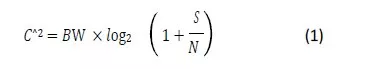
where C is the channel capacity, BW is the bandwidth of the channel, S and N are the averaged signal power and averaged noise power, respectively. The capacity to transmit information, C, is directly proportional to channel bandwidth, implicating that exceeding growth in transmitted data over a communications channel would also increase the bandwidth demand.
In a wireless system like the 5G today (and the future 6G), to support carrier aggregation and allow for more efficient use of the available spectrum, the RF front end including data converter must be able to handle a wide signal bandwidth that encompasses all the frequency bands being used. The signal bandwidth requirement will vary depending on the specific configuration and the frequency bands being used and in general, the bandwidth is then wider when carrier aggregation or Digital-Pre-Distortion (DPD) are implemented.
Sampling Frequency and Resolution
High sampling frequency is a key parameter driving the capability for direct RF sampling approach. With appropriate selection of the sampling frequency, the desired RF band can be shifted farther away from the Nyquist frequency, thus, reducing the risk of aliasing, increasing fidelity and accuracy of the digitized signal.
Additionally, it provides a greater resolution of the spectral content of the input signal. With this increased resolution, the signal processing principles can more accurately separate the wanted transmission from the adjacent channel signals, even when their sidebands overlap and diminish the level of interference, resulting in a higher quality output.
When employing direct RF sampling, the effect on the sensitivity of the receiver is necessary to be considered. To improve sensitivity, the overall noise floor must be at an optimal level which translates into reducing the errors introduced by quantisation and jitter.
Hardware Design Optimization
Eliminating traditional analogue requirements and the IF stage in direct RF sampling converters simplifies hardware design, offering several benefits. By minimising the number of components and reducing circuit complexity, the overall size of the system is significantly decreased, making it more accessible and practical for a wider range of applications. A simplified design can also be easier to manufacture and maintain, leading to increased reliability and reduced downtime.
Optimising the hardware can improve performance and signal quality by reducing potential sources of noise and distortion. Without a mixer, there are no mixing images or local oscillator spurious signals to worry about, resulting in a cleaner and more accurate signal. This technology is particularly advantageous for solutions with small size and high integration requirements, such as in today’s 5G applications.
However, it's important to consider the potential upfront costs associated with developing such RF data converters. If the target IPs are not available on the market due to specific performance requirements (e.g., WiFi 7 and 6G), the development process may require a significant investment in highly specialised engineers to design and verify these IPs. The development may also necessitate multiple test chip tape-outs to confirm that the overall design functionality and performance meet specifications before final integration into the System on Chip (SoC) or chiplet.
Digital Integration
Improvement in Fin-FET process technologies has enabled the incorporation of more complex digital control circuits alongside the analogue RF front-end. An area of increased prominence, especially considering 6G, is the integration of advanced features such as adaptive equalisation and machine learning (ML) algorithms which can help to compensate for signal distortions caused by transmission through different media.
ML approaches due to their ability can achieve more precise calibration by recognising the imperfections of the system and rectifying them in real-time. They can also allow for more agile and adaptive systems that can be reconfigured to meet changing requirements or operating conditions.
An example of such applications is the implementation of Artificial Intelligence (AI) in conjunction with Digital Pre-Distortion (DPD) to alleviate distortion in the transmitter path of a wireless communication system. By using artificial neural networks (ANN), it is possible to build more accurate models of the nonlinearities in the transmitter, allowing for more effective pre- distortion. These technologies are becoming increasingly prominent in technical papers presented by researchers in the wireless field.
I/O Flexibility
In addition to delivering Giga-sample-per-second (GSPS) capability, the new class of RF sampling architecture accommodates high speed serial interface. The use of a low power, multigigabit serial interface as the bridge for communication between the converter and digital processor can result in more power-efficient and compact digital interconnect. The I/O flexibility of RF sampling data converters was greatly enhanced by the JESD204B standard in recent years, which permitted the transmission of digital input/output data at high lane rates of up to 12.5 Gbps per lane, providing a significant degree of flexibility. The current standard, the JESD204C, supports up to 32Gbps per lane providing improved features for synchronisation and data packing. The next advancement is the JESD204D standard, which supports PAM4 data rates up to 116Gbps and NRZ up to 58Gbps. However, no publicly available solutions currently support this standard.
Chiplet and UCIe
In addition to the usual standalone devices with SerDes interface, the new foreseen trend is chiplet. The chiplet, as general definition, is an IC that is specialised in a specific function and can be interconnected to other chiplets using the Die-to-Die (D2D) interface. The new designs of chiplets have been mainly using Bunch of Wires (BoW) and Universal Chiplet Interface Express (UCIe) with the last one being seen as the future standard. The new RF transceivers that will be coming onto the market in chiplet form in the next few years will need to use these interfaces and still maintain the key functionalities such as synchronisation, deterministic latency and low power consumption.
Challenges for Effective Implementation
While direct RF sampling approach offers notable advantages, it is important to acknowledge the associated challenges and trade-offs that come with this RF architecture.
Power Dissipation
The primary consideration is that RF converters consume a substantial amount of power.
Operating at higher sampling rate can pose a challenge in terms of dynamic power dissipation which is dependent on the number of times a capacitor is charged and discharged. Hence, as the switching frequency increases, the dissipated power also increases correspondingly. This correlation can be expressed as:

with f being the switching frequency and CL the load capacitance for a CMOS.
Another factor to consider is that higher frequency signals require more slew rate to accurately capture their fast transitions. This requirement necessitates having more DC gain particularly as the signal amplitude increases along the signal path which subsequently cause more power dissipation in RF sampling data converters.
There is often a compromise between power consumption and performance in data converters. Eq. (3) quantifies the converter's performance efficiency by considering the ENOB achieved at a given sampling frequency relative to the power consumed:

where Pdissp indicates the dissipated power, FOM is the figure of merit, fs and ENOB are sampling rate and effective number of bits, respectively.
Design choices that prioritize power efficiency may lead to lower sampling rates or lower ENOB, while maximising performance may result in higher power consumption.
It is worth noting that eq. (3) only refers to power consumption of the data converter, hence, powers associated with other circuitries need to be addressed independently.
Gain Distribution
In RF sampling data converters, it is vital to have a relatively flat gain response across the entire operating frequency range. This is important to preserve the amplitude information of the RF signals with fidelity. Achieving a flat gain response can be challenging due to the potential impact of frequency-dependent gain variations caused by analogue front-end components.
Clock and Timing
Precise clock and timing distribution is another major concern in high-speed RF converters to ensure accurate sampling and synchronisation. Modern applications such as Wi-Fi 7 with 4096K QAM modulation and channel bandwidth up to 320MHz impose a great challenge to meet increasingly stringent requirements of high dynamic range over a wide bandwidth and eliminate any possible SNR/SFDR degradation.
In addition to aperture jitter of the converter itself, jitter in any scenario is originated from multiple sources, ranging from oscillator and frequency dividers to clock buffers and noise induced by coupling effects.
To further demonstrate the impact of clock jitter on the data converter performance, mathematical estimation of Signal-to- Noise Ratio (SNR) for a given value of jitter is presented as:

Eq. (4) is derived presuming a sinusoidal input signal with frequency fin and considering a Gaussian distribution with zero mean and standard deviation of σ for jitter. As it can be inferred from eq. (4), for a fixed amount of jitter SNR deteriorates as the input frequency increases.
Various techniques are employed to mitigate clock jitter, including low-noise clock sources, careful PCB layout and grounding, shielding, and filtering techniques to reduce noise coupling as well as advanced clock conditioning and synchronisation techniques.
Process Technology
As mentioned already, the process node plays a key role in the direct RF solution. The analogue power required to keep the same level of performance doesn’t scale with the process technology. The lowest nodes also show higher complexity to get the same level of analog performance sometime at expense of higher power consumption. The digital design, continuously increasing in feature set is, instead, taking full advantage of the newest nodes. The reality is that any team today approaching the design of these solutions will try to find the right compromises between cost, power, performance and feature set although, sometimes, the decision is driven mainly by customers and market.
The other case where the converters are integrated in complex digital asic, the overall analogue power is sometimes nowhere comparable with the overall digital power of the entire SoC. In this situation, a monolithic design in the lower node might be the right decision power wise. It is also now highly probable that the best solution will be based on a chiplet architecture that will be the perfect example of how to split digital and analog functions in different ICs and using UCIe to interconnect the two worlds.
Modern Usage and Applications
The launch of 3GPP Release 18 signifies another major evolution in 5G technology, propelling the industry towards the era of 5G-Advanced. To fulfil the rigorous specification of post-5G era and forthcoming wireless communication systems, there is a growing need in incorporating technologies such as Massive Multiple-Input Multiple-Output (mMIMO), beamforming, sub-millimeter wave, and Tera-hertz spectrum as the integral components.
Massive MIMO, one of the main enablers of 5G New Radio (NR), exploits a large number of antenna elements along with spatial diversity and spatial multiplexing to transmit multiple parallel data signals. Expanding the number of channels within the available spectrum enhances network capacity and enables faster data throughput to each individual user.
The implementation of RF front ends, including data converters, holds a significant importance in these networks due to the requirement of numerous antenna elements at the base stations. By leveraging direct RF sampling, mMIMO systems can achieve considerable reduction in design complexity, smaller form factors, enhanced integration with antennas, and simplified deployment and maintenance. These benefits contribute to the scalability, efficiency, and performance of mMIMO technology in delivering high-capacity wireless communication systems, as well as enabling complex digital features such as full digital beamforming functionality.
Direct RF sampling offers an additional advantage of a less complex RF signal chain, resulting in reduced cost per channel. By consolidation of multiple analogue components into a more streamlined architecture, systems adopting direct RF are often more compact and energy efficient. For applications such as phased-array radar which often require many antennas ranging from hundreds to thousands for beamforming and spatial processing, direct RF sampling can effectively decrease the overall size, power consumption and cost of the system.
Moreover, by utilizing direct RF sampling, more simplified synchronization can be realized. To attain phase coherence within an RF system and allow for accurate and reliable data transmission, it is essential to make certain that internal clocks and local oscillators of the devices are precisely aligned. However, with direct sampling, which eliminates the need for LOs, the focus shifts solely to clock synchronization. This yet again can be particularly advantageous for phased-array radar applications where maintaining phase coherence among multiple RF receivers is crucial.
To provide enhanced wireless connectivity and ensure optimal network performance, a 5G Radio Access Network (RAN) relies on a highly coordinated, multi-layer network that encompasses low-band, mid-band, and high-band frequencies.
Another key benefit of direct RF sampling is the ability to accurately position channels within the analogue bandwidth, offering precise channel allocation flexibility.
In future generations of wireless systems like 6G, a further increase of direct RF sampling channel is expected. Back in February 2024 a 4096 element mMIMO array covering FR3 bands (10GHz-15GHz) has been shown and it is expected in the next 15-24 months the first commercial solutions to be available.
Conclusion
Advanced RF technologies pave the way for progressive applications such as Software Defined Radio (SDR), Beamforming, Phased Array Radars, Open Radio Access Networks (O-RAN), V2X and Internet of Things (IoT) which subsequently drive the demand for high-speed radio frequency converters with high precision and size, weight, and power (SWaP) requirements. These solutions will now start taking advantage of the new chiplet ecosystem being built and developed around the idea of complex die disaggregation towards a ‘functional’ die strategy with optimum size, cost, area and process. In the future it is foreseeable to see more and more RF chiplet based solutions in every market including Telecom, Industrial, Automotive and IoT.
References
- [1] Tommy Neu, Texas Instruments, White Paper, May 2015: “Direct RF conversion: From vision to reality”. Available online: Direct RF conversion: From vision to reality
- [2] D. Siafarikas and J. L. Volakis, "Toward Direct RF Sampling: Implications for Digital Communications.", IEEE Microwave Magazine, vol. 21, no. 9, pp. 43-52, Sept. 2020.
- [3] D. Li, et al., “Radio frequency analog-to-digital converters: Systems and circuits review.”, Microelectronics Journal, Volume 119, 2022.
- [4] A. Mashhour, et al., “On the Direct Conversion Receiver—A Tutorial,” Microwave Journal, June 2001.
- [5] “An Adaptable Direct RF-Sampling Solution”, Xilinx, February 2019. Available online: Direct RF-Sampling Solution
- [6] Brad Brannon. “Radio Architecture Matters: A Review of RF Sampling vs. Zero-IF.”, Analog Devices, Inc.
- [7] R. H. Walden, "Analog-to-digital converter survey and analysis," in IEEE Journal on Selected Areas in Communications, vol. 17, no. 4, pp. 539-550, April 1999, doi: 10.1109/49.761034.
- [8] M. Shinagawa, Y. Akazawa and T. Wakimoto, "Jitter analysis of high-speed sampling systems," in IEEE Journal of Solid-State Circuits, vol. 25, no. 1, pp. 220-224, Feb. 1990, doi: 10.1109/4.50307.
- [9] R. H. Walden, "Analog-to-digital converter survey and analysis," in IEEE Journal on Selected Areas in Communications, vol. 17, no. 4, pp. 539-550, April 1999, doi: 10.1109/49.761034.
- [10] P. Delos, “Advanced Technologies Pave the Way for New Phased Array Radar Architectures” Analog Devices, Inc.
- [11] “Advantages of Direct RF Sampling Architectures.” National Instruments September 2022, Available online: Advantages of Direct RF Sampling Architectures
- [12] J. Crowe, Barrie Hayes-Gill, “Introduction to Digital Electronics.” Newnes, 1998, Pages 191-239, ISBN 9780340645703.
- [13] J. Wannstrom, “Carrier Aggregation explained.”, 3GPP, Dec ,2022. 2017. Available online: Carrier Aggregation Explained
- [15] 3GPP Release 18, Available online: Release 18
ABOUT ANALOGUE INSIGHT
Established in early 2024, at Analogue Insight, we are Bridging the Analogue and Digital Worlds for Tomorrow's through our Chiplet Solutions. Our core expertise lies in developing cutting-edge Chiplet technology that serves as the building block for advanced communication systems.
Our Chiplets are designed to offer high performance, scalability, and integration flexibility, enabling our clients to achieve breakthroughs in computation speed, data processing, and connectivity. Get in contact and discover how our Chiplet solutions can transform your projects and operations.
To learn more, visit: analogueinsight.com
Reach out to us at: info@analogueinsight.com
Related Chiplet
- DPIQ Tx PICs
- IMDD Tx PICs
- Near-Packaged Optics (NPO) Chiplet Solution
- High Performance Droplet
- Interconnect Chiplet
Related Technical Papers
- Temporary Direct Bonding by Low Temperature Deposited SiO2 for Chiplet Applications
- Stop-For-Top IP model to replace One-Stop-Shop by 2025... and support the creation of successful Chiplet business
- Chiplet Strategy is Key to Addressing Compute Density Challenges
- RapidChiplet: A Toolchain for Rapid Design Space Exploration of Chiplet Architectures
Latest Technical Papers
- Link Quality Aware Pathfinding for Chiplet Interconnects
- Effects of Poor Workload Partitioning on System Performance for Chiplet-Based Systems
- Mozart: Modularized and Efficient MoE Training on 3.5D Wafer-Scale Chiplet Architectures
- Network Design for Wafer-Scale Systems with Wafer-on-Wafer Hybrid Bonding
- CarbonPATH: Carbon-aware pathfinding and architecture optimization for chiplet-based AI systems