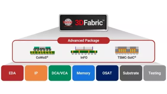
After TSMC fab in Japan, advanced packaging facility is next
By Majeed Ahmad, EDN (March 18, 2024)

 Japan’s efforts to reboot its chip industry are likely to get another boost: an advanced packaging facility set up by TSMC. That seems a logical expansion to TSMC’s $7 billion front-end chip manufacturing fab built in Kumamoto on Japan’s southern island Kyushu.
In other words, a back-end packaging facility will follow the front-end fab to complement the chip manufacturing ecosystem in Japan amid considerations to diversify semiconductor supply chains beyond Taiwan due to geopolitical tensions. Trade media has been abuzz about TSMC setting up an advanced packaging plant and a new Reuters report supports this premise.
To read the full article, click here
Related Chiplet
- DPIQ Tx PICs
- IMDD Tx PICs
- Near-Packaged Optics (NPO) Chiplet Solution
- High Performance Droplet
- Interconnect Chiplet
Related News
- SK hynix Signs Preliminary Memorandum of Terms with U.S. Department of Commerce for Advanced Packaging Facility in Indiana
- Amkor and TSMC to Expand Partnership and Collaborate on Advanced Packaging in Arizona
- Silicon Box welcomes European Commission approval of €1.3 billion Italian State aid measure to support new advanced packaging facility in Novara
- Nvidia, TSMC, and advanced packaging realignment in 2025
Latest News
- NLM Photonics Samples Silicon Organic Hybrid PICs Manufactured at GlobalFoundries
- Avalanche Technology and NHanced Semiconductors Leverage Advanced 2.5D Integration to Bring Optimal SWaP and Reliability to Rad-Hard FPGAs
- Open EU Foundry status granted to innovative chiplet facility
- Siluxtek and GlobalFoundries Forge a Deep Strategic Partnership to Mass-Produce 200G/Lane Silicon Photonic Receiver Chips, Paving the Way for the Industrial Revolution of AI Computing Interconnects
- Lightwave Logic High-Speed Modulator Platform Now Available in GDS Factory PDK for GlobalFoundries Silicon Photonics Platform