India’s OSAT Ambitions: Flying High or a Flight Risk?
By Yashasvini Razdan, EETimes | May 19, 2025
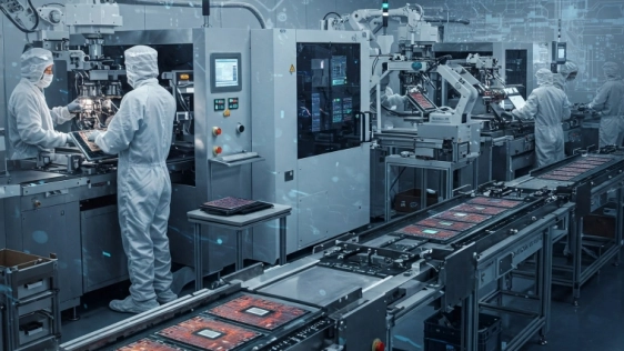
Until a few years ago, semiconductors were the nerds of the tech class—omnipresent yet inconspicuous. But over the past decade, and especially since the global chip shortage, the spotlight has finally landed on the backbone of the modern tech economy. India, long known for its IT services, wants in on the hardware action.
Government subsidies are pouring in, timelines are being set and large players are building facilities in India that aim to rival Southeast Asian giants.
The Indian government has formally approved four OSAT/ATMP (assembly, testing, marking and packaging) units and one full-fledged fabrication facility under the Semicon India Program, spearheaded by the India Semiconductor Mission. The goal is clear: to become a meaningful player in the global semiconductor supply chain. Collectively, these projects represent a cumulative investment of ₹1.52 (approximately $18.2 billion) and are expected to be completed over the next four to six years.
To read the full article, click here
Related Chiplet
- Interconnect Chiplet
- 12nm EURYTION RFK1 - UCIe SP based Ka-Ku Band Chiplet Transceiver
- Bridglets
- Automotive AI Accelerator
- Direct Chiplet Interface
Related News
- Micross Acquires Integra Technologies, Creating the Leading U.S. Domiciled OSAT Provider
- Veeco Announces Over $35 Million in Advanced Packaging Lithography System Orders From IDM & OSAT Customers
- Top 10 OSAT Companies of 2024 Revealed—China Players See Double-Digit Growth, Reshaping the Global Market Landscape, Says TrendForce
- Siemens expands OSAT Alliance membership to build domestic semiconductor supply chains
Latest News
- PulseForge Announces Availability of PD700 SA – A Semi-Automated Photonic Debonding Tool Optimized for Large-Panel Advanced Packaging
- Global Semiconductor Equipment Sales Projected to Reach a Record of $156 Billion in 2027, SEMI Reports
- Strategic alignment between imec and Japan’s ASRA aims to harmonize standardization of automotive chiplet architectures
- TOPPAN to Install Pilot Line for Advanced Semiconductor Packaging at Ishikawa Plant
- CHASSIS: European mobility, semiconductor, and software heavyweights team up with research in joint initiative for automotive chiplet technology