PulseForge Announces Availability of PD700 SA – A Semi-Automated Photonic Debonding Tool Optimized for Large-Panel Advanced Packaging
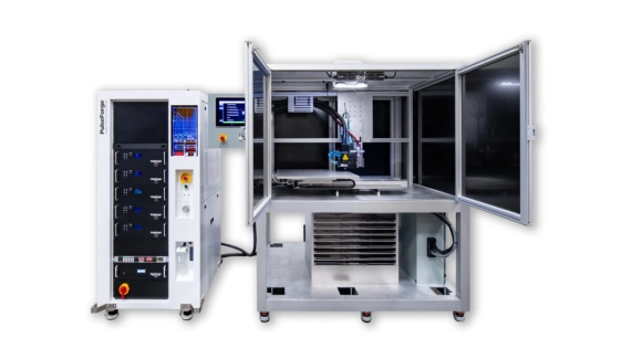
Austin, TX – December 16, 2025 – PulseForge, Inc., the exclusive provider of photonic debonding technology, today announced the release and commercial availability of the PD700 SA, a semi-automated photonic debonding tool engineered specifically for large-panel-level packaging semiconductor manufacturing. The new system supports substrate sizes up to 700 mm x 700 mm.
 Targeted toward manufacturers of AI chips, 2.5D/3D architectures, interposers, silicon photonics, and next-generation heterogeneous integration, the PD700 SA delivers a bridge platform between process evaluation and high-volume production, enabling customers to validate speed, reliability, and cost-efficiency before full-scale deployment.
The PD700 SA directly addresses the industry’s transition to panel-level manufacturing driven by surging AI and HPC demand. Key advantages include:
- True panel-level operation up to 700 mm × 700 mm in the same tool
- Zero-stress, warp-tolerant debonding for fragile and bowed panels
- Multi-size substrate compatibility for maximum production flexibility
- Ultra-fast cycle times with minimal thermal load
- Lower cost-of-ownership (CoO) versus laser, thermal, or mechanical debonding
Superior Performance for Advanced Packaging
“The PD700 SA extends PulseForge’s leadership in photonic debonding for large-panel-level photonic debonding,” said Jonathan Gibson, CEO, PulseForge, Inc. “This tool was engineered in direct collaboration with leading semiconductor manufacturers, and materials partners as bridge between early-stage evaluation and high-volume production to meet the growing demand for panel-level interposer production.”
Target Applications
The PD700 SA is ideally suited for manufacturers working on:
- Artificial Intelligence (AI) and HPC chip packaging
- TSV interposer fabrication
- Glass and organic panel-level interposers
- 2.5D, 3D, and emerging 3.5D architectures
- Super-large panels for CoPoS-class systems
The PD700 SA is available for immediate order, with first shipment planned in, December 2025 to Resonac Corporation. Resonac corporation is leading the panel-level interposer manufacturing development through its Joint3 efforts. For demonstrations and sample processing please contact PulseForge at pf.sales@pulseforge.com.
About PulseForge
PulseForge, Inc. develops and manufactures state-of-the-art flashlamp-based tools that deliver energy in a precise and targeted manner to enable innovation in industrial manufacturing. Our expertise and tools empower our customers to explore novel materials and manufacturing methodologies, driving dynamic and efficient production at an industrial scale.
Related Chiplet
- Interconnect Chiplet
- 12nm EURYTION RFK1 - UCIe SP based Ka-Ku Band Chiplet Transceiver
- Bridglets
- Automotive AI Accelerator
- Direct Chiplet Interface
Related News
- Resonac and PulseForge Unite to Advance Photonic Debonding for Next-Gen Semiconductor Packaging
- Enosemi and Jabil to develop advanced packaging process technology for photonic chips
- PulseForge Achieves Record Photonic Debonding Orders in Q1 2025, Signaling Market Acceleration
- GlobalFoundries Announces New York Advanced Packaging and Photonics Center
Latest News
- PulseForge Announces Availability of PD700 SA – A Semi-Automated Photonic Debonding Tool Optimized for Large-Panel Advanced Packaging
- Global Semiconductor Equipment Sales Projected to Reach a Record of $156 Billion in 2027, SEMI Reports
- Strategic alignment between imec and Japan’s ASRA aims to harmonize standardization of automotive chiplet architectures
- TOPPAN to Install Pilot Line for Advanced Semiconductor Packaging at Ishikawa Plant
- CHASSIS: European mobility, semiconductor, and software heavyweights team up with research in joint initiative for automotive chiplet technology