How the Worlds of Chiplets and Packaging Intertwine
By Majeed Ahmad, EETimes (September 26, 2023)
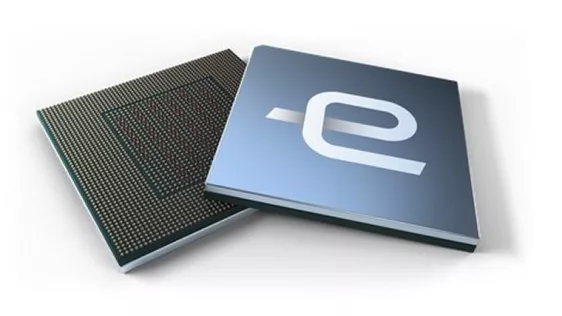
Chiplets mark a new era of semiconductor innovation, and packaging is an intrinsic part of this ambitious design undertaking. However, while chiplet and packaging technologies work hand in hand to redefine the possibilities of chip integration, this technological tie-up isn’t that simple and straightforward.
In chip packaging, the bare chip die is encapsulated in a supporting case with electrical contacts. The case protects the bare die from physical harm and corrosion and connects the chip to a PCB. This form of chip packaging has existed for decades.
To read the full article, click here
Related Chiplet
- Interconnect Chiplet
- 12nm EURYTION RFK1 - UCIe SP based Ka-Ku Band Chiplet Transceiver
- Bridglets
- Automotive AI Accelerator
- Direct Chiplet Interface
Related News
- Chiplets: Piecing Together the Next Generation of Chips (Part I)
- Alphawave Semi to Reveal Ecosystem and Key Architectures Unlocking Generative AI Potential at EE Times' "Chiplets: Building the Future of SoCs" Seminar
- Chiplets: Piecing Together the Next Generation of Chips (Part II)
- ACM Research Enters Fan-out Panel Level Packaging Market with Introduction of Ultra C vac-p Flux Cleaning Tool for Chiplets
Latest News
- Cadence Launches Partner Ecosystem to Accelerate Chiplet Time to Market
- Ambiq and Bravechip Cut Smart Ring Costs by 85% with New Edge AI Chiplet
- TI accelerates the shift toward autonomous vehicles with expanded automotive portfolio
- Where co-packaged optics (CPO) technology stands in 2026
- Qualcomm Completes Acquisition of Alphawave Semi