Advanced Packaging Drives New Memory Solutions for the AI Era
Lam Research’s advanced packaging breakthroughs enable fast, high-bandwidth memory for the AI-everywhere world
By Lam Research (September 19, 2024)
From self-driving cars to advanced data analysis, the continuing growth of artificial intelligence (AI) applications has significantly changed the demands for computing power and memory. AI technologies require extensive computational capabilities and rapid data processing. This puts increasing pressure on the underlying hardware to deliver improved performance.
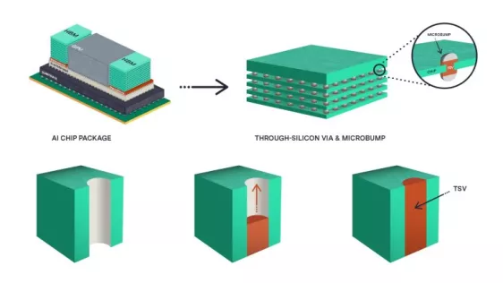
Innovative solutions in memory and processing architecture are needed – most notably, high-bandwidth memory (HBM) enabled by advanced packaging.
Traditional chip design limitations highlight the importance of advanced packaging
Historically, chip design advancements have followed Moore’s Law, which predicted that the number of transistors on a microchip would double approximately every two years, leading to improved performance. However, this trend is facing physical and technical limitations.
Conventional chip designs must be revamped to meet AI’s high-speed data transfer and low-latency demands. These limitations drive the semiconductor industry to explore advanced packaging solutions that can integrate multiple chips into a single package, enhancing performance and efficiency while extending Moore’s Law.
To read the full article, click here
Related Chiplet
- DPIQ Tx PICs
- IMDD Tx PICs
- Near-Packaged Optics (NPO) Chiplet Solution
- High Performance Droplet
- Interconnect Chiplet
Related News
- SCHMID Group Expands Advanced Packaging Portfolio to Power the AI Era
- Silicon Box Ships 100M Units, Proves Advanced Panel-Level Packaging Ready for AI, HPC era
- KLA Unveils Comprehensive IC Substrate Portfolio for a New Era of Advanced Semiconductor Packaging
- ISE Labs Investment Secures the Establishment of New Site for Semiconductor Packaging and Test in Mexico
Latest News
- Agileo Automation Launches Agil'EDA to Accelerate SEMI EDA Adoption for Semiconductor Equipment OEMs
- AEM and ASE Enter Strategic Partnership to Accelerate AI and HPC Test Innovation
- NLM Photonics Samples Silicon Organic Hybrid PICs Manufactured at GlobalFoundries
- Avalanche Technology and NHanced Semiconductors Leverage Advanced 2.5D Integration to Bring Optimal SWaP and Reliability to Rad-Hard FPGAs
- Open EU Foundry status granted to innovative chiplet facility