A methodology for turning an SoC into chiplets
By Nick Flaherty, eeNews Europe (July 25, 2023)
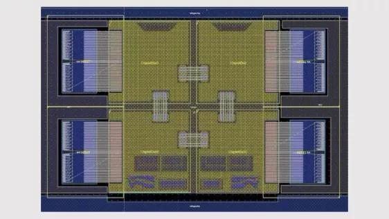
Siemens has developed a workflow methodology for homogeneous disaggregation of SoCs into chiplets using hierarchical device planning.
The key benefit of adopting hierarchy inside of a design is clear – a seemingly large and complex designs can be disaggregated into smaller and easier to manage building blocks based on a collection of attributes such as function and position.
Advancements in IC packaging manufacturing, combined with the exploding costs of designing monolithic ICs on today’s advanced process nodes, have given rise to a growing trend of disaggregating large SoCs into smaller dies and chiplets says Chris Cone at Siemens EDA.
This increased design complexity requires iterative multi-physics analysis during the floorplanning stage and optimization of the design for PPA and cost goals, significantly raising the barrier for project success. Trying to employ traditional package design solutions – where each device is modeled as a single flat entity – is time consuming and unnecessarily risks delaying production.
However many design structures are comprised of repeatable patterns that can be represented as a parameterized object which is a form of hierarchical design capture. In IC packaging there are two key classes of design structures which lend easily to incorporating hierarchy – these are die-to-die signal interfaces and power distribution networks.
To read the full article, click here
Related Chiplet
- DPIQ Tx PICs
- IMDD Tx PICs
- Near-Packaged Optics (NPO) Chiplet Solution
- High Performance Droplet
- Interconnect Chiplet
Related News
- Avnet ASIC and Bar-Ilan University Launch Innovation Center for Next Generation Chiplets
- BOS Semiconductors Signed Development Contract for ADAS Chiplet SoC with an European OEM
- What could back an open market for chiplets?
- Cadence Accelerates SoC, 3D-IC and Chiplet Design for AI Data Centers, Automotive and Connectivity in Collaboration with Samsung Foundry
Latest News
- Lightmatter Introduces Guide Light Engine for AI, Featuring VLSP Technology
- Lightmatter and GUC Partner to Produce Co-Packaged Optics (CPO) Solutions for AI Hyperscalers
- Lightmatter Collaborates with Synopsys to Integrate Advanced Interface IP with Its Passage Co-Packaged Optics Platform
- Lightmatter and Cadence Collaborate to Accelerate Optical Interconnect for AI Infrastructure
- Hybrid Bonding Comes of Age Slowly and Collectively