€2.5bn for European 1nm chiplet pilot line at imec
By Nick Flaherty, eeNews Europe (May 21, 2024)
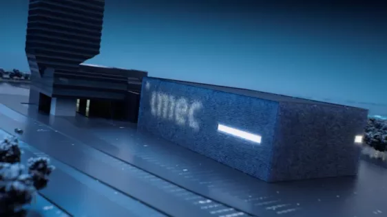
imec in Belgium is to host a pilot line to develop 1nm CMOS SoC and chiplet technologies with an investment of €2.5bn.
The NanoIC pilot line will focus on sub-2nm CMOS technology, which will be key for the Intel 16A process with features as small as 1.6nm and below. Prototyping chiplets is expected to be a key technology for the line.
The funding was announced at the imec technology forum (ITF) in Antwerp today with €1.4bn expected to come from Horizon Europe and Digital Europe through the Chips Joint Undertaking(Chips JU) and the Flanders state government.
However the grant agreement with the Chips JU is currently ongoing and is expected to be signed later this year. This is one several pilot lines covered in eeNews Europe in April, including one for FD-SOI low power process technologies at CEA-Leti in Grenoble: Four pilot lines for the EU chip joint undertaking
Leti is also a partner in the NanoIC pilot line along with Fraunhofer-Gesellschaft in Germany, VTT in Finland, CSSNT in Romania and the Tyndall Institute in Ireland.
To read the full article, click here
Related Chiplet
- Interconnect Chiplet
- 12nm EURYTION RFK1 - UCIe SP based Ka-Ku Band Chiplet Transceiver
- Bridglets
- Automotive AI Accelerator
- Direct Chiplet Interface
Related News
- Imec achieves seamless InP Chiplet integration on 300mm RF Silicon Interposer with excellent performance at 140GHz
- GlobalFoundries, Infineon, Silicon Box, STATS ChipPAC, TIER IV Join imec Automotive Chiplet Program
- Imec inaugurates its Baden-Württemberg office, focused on advancements in automotive chiplet
- Strategic alignment between imec and Japan’s ASRA aims to harmonize standardization of automotive chiplet architectures
Latest News
- Qualcomm Completes Acquisition of Alphawave Semi
- Cadence Tapes Out UCIe IP Solution at 64G Speeds on TSMC N3P Technology
- Avnet ASIC and Bar-Ilan University Launch Innovation Center for Next Generation Chiplets
- SEMIFIVE Strengthens AI ASIC Market Position Through IPO “Targeting Global Markets with Advanced-nodes, Large-Die Designs, and 3D-IC Technologies”
- FormFactor Expands Silicon Photonics Test Capabilities With Acquisition of Keystone Photonics