Intel and Alphawave Semi Demonstrates UCIe Interoperability
Chiplets bring several advantages in terms of cost, performance and yield, but among the key benefits is the ability to enact multi-vendor chiplet ecosystems. In these, chiplets from a range of vendors, each built using the optimal process node for that function can work together seamlessly in a SiP (System in a Package). But this is only true when we have a standard, open (i.e. non-proprietary) die-to-die communication protocol.
Universal Chiplet Interconnect Express (UCIe) provides that common standardized interface for chiplets to communicate regardless of the vendor, foundry, or process node. It provides design flexibility over form factors, such as the use of organic substrate standard packaging, advanced packaging with silicon interposer, RDL, bridge type solutions, or 3D hybrid bonding. Critically, this interoperability allows elements within chiplet-based designs to be easily swapped out and/or upgraded without a redesign of the entire system.
In this paper we will provide an overview of the scenarios covered in an Intel and Alphawave Semi UCIe interoperability demonstration. Stimulus was provided by Intel UCIe standard package PHY and received by Alphawave’s UCIe PHY. The bring-up process of PHY parameters was constrained by specific configurations of clock modes, data rates, and other UCIe technical specifications that ensure proper system function. The multi-module bring-up requirements and states from the link training state machine (LTSM) were covered during the training phases.
Overview of Design Verification Setup for Interoperability Testing
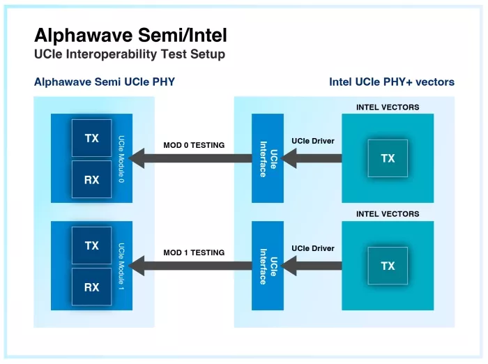
Figure 1: Design Verification Setup and placement of vectors for Alphawave Semi and Intel UCIe PHYs interoperability testing
As we can see in the above figure 1, the Intel vectors containing sideband and mainband signals are being driven to a UCIe DUT interface by Alphawave Semi’s UCIe driver. These signals are driven to design RX via the UCIe interface. The design simulates and sends the response over the UCIe interface to bring up the LTSM.
PHY Parameters Constrained During UCIe Bring-Up
During the UCIe bring-up phase, several PHY parameters were constrained to ensure proper system function and configuration. The table below outlines these parameters, and the range of acceptable configurations.
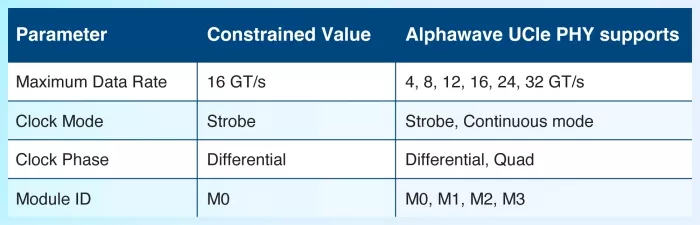
Detailed Parameter Breakdown
- Maximum Data Rate: Constrained to 16 GT/s during bring-up but UCIe PHY can support a wider range between 4 to 32 GT/s depending on system configuration.
- Clock Mode: Strobe mode is used during the bring-up, but a continuous clock mode is available in other scenarios.
- Clock Phase: Differential clock phase is constrained, while quad-phase configurations are excluded.
- Module ID: Bring-up occurs with a single UCIe module (M0), while other modules (M1-M3) are also successful in the standard process of link state bring-up.
Multi-Module Bring-Up Requirements
At this point, it should also be noted that when bringing up multiple modules, Intel stimulus required separate vectors for each module. Each vector must be associated with a distinct Module ID. System bring-up for multiple modules was successfully covered by Intel stimulus by instantiating the same Intel vectors for each module. Some of the LTSM states required from reset to an active die-to-die link are described below.
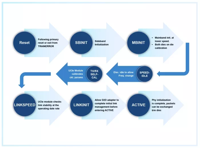
Figure 2: UCIe LTSM States
Results and Achievements
The collaborative interoperability testing between Intel and Alphawave Semi yielded several significant achievements.
- Firstly, the testing accomplished the bring up of the UCIe link, which includes sideband and mainband signals bring up.
- Data integrity was also demonstrated, with the LFSR (Linear Feedback Shift Register) pattern sent over mainband during LINKSPEED state.
- Timing was synced with design behavioral models and the vectors to bring up LTSM within 40 µs.
- Furthermore, during the process, the design under test (DUT) was able to seamlessly bring up the state machine with 0 new bugs found.
- Specifically, we learned both that the vectors contained mainband clock and valid glitches to mimic real time scenario, and that the DUT was able to handle it.
- And using the data provided in the Intel vectors, we developed an understanding on how to synchronize its timing with the DUT to for better simulations.
Identified challenges and lessons learned for UCIe Interoperability
The interoperability testing also highlighted several challenges and provided valuable lessons for future UCIe ecosystem development.
- As part of this team-effort, several issues were identified and resolved for the successful interoperability between Intel and Alphawave Semi UCIe PHY IPs. These were primarily related to the three following groups:
- Some unintentional mainband valid bit-slips in vectors.
- Valid and clock alignment issue on mainband signals.
- And shifts in the lane id pattern sent during bring up.
- The results and analysis also showed areas to improve the dataset, notably that it’s possible to provide vectors with a smaller delay to ensure greater exactness for these vectors.
- Additionally, Alphawave Semi provided a list of additional PHY parameters for inclusion in Intel vectors to test interoperability for all scenarios such as clock mode in future testing.
Conclusion
Intel UCIe PHY stimulus played a critical role in the UCIe link bring-up and interoperability process of the Alphawave Semi UCIe PHY. The UCIe modules demonstrated stability of the die-to-die link after the reset, sideband, and mainband training and calibration processes were performed.
In conclusion, this demonstration of interoperability between the Intel and Alphawave Semi UCIe PHY through simulation addresses the enablement of successful and robust die-to-die communication in a broader multi-vendor open chiplet ecosystem.
Related Chiplet
- DPIQ Tx PICs
- IMDD Tx PICs
- Near-Packaged Optics (NPO) Chiplet Solution
- High Performance Droplet
- Interconnect Chiplet
Related Blogs
- Unleashing Die-to-Die Connectivity with the Alphawave Semi 3nm 24Gbps UCIe Solution
- UCIe for 1.6T Interconnects in Next-Gen I/O Chiplets for AI data centers
- Alphawave Semi Bridges from Theory to Reality in Chiplet-Based AI
- Advancing the Open Chiplet Ecosystem with UCIe 2.0
Latest Blogs
- Advancing High‑Performance Silicon Photonics and Silicon Germanium (SiGe) for the Next Era of Optical Connectivity
- Accelerating Chiplet Innovation with a New Partner Ecosystem
- Accelerating Multi-Die Innovation: How Synopsys and Samsung are Shaping Chip Design
- Six critical trends reshaping 3D IC design in 2026 and beyond
- AI Energy Gap and Chiplets: Why Data Movement Matters