HexaMesh: Scaling to Hundreds of Chiplets with an Optimized Chiplet Arrangement
By Patrick Iff ∗, Maciej Besta ∗, Matheus Cavalcante †, Tim Fischer †, Luca Benini †‡ and Torsten Hoefler ∗
∗ Department of Computer Science, ETH Zurich, Zurich, Switzerland
† Department of Information Technology and Electrical Engineering, ETH Zurich, Zurich, Switzerland
‡ Dept. of Electrical, Electronic and Information Engineering, University of Bologna, Italy
Abstract
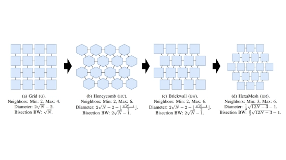
2.5D integration is an important technique to tackle the growing cost of manufacturing chips in advanced technology nodes. This poses the challenge of providing high-performance inter-chiplet interconnects (ICIs). As the number of chiplets grows to tens or hundreds, it becomes infeasible to hand-optimize their arrangement in a way that maximizes the ICI performance. In this paper, we propose HexaMesh, an arrangement of chiplets that outperforms a grid arrangement both in theory (network diameter reduced by 42%; bisection bandwidth improved by 130%) and in practice (latency reduced by 19%; throughput improved by 34%). HexaMesh enables large-scale chiplet designs with high-performance ICIs.
To read the full article, click here
Related Chiplet
- eFPGA Chiplet
- DPIQ Tx PICs
- IMDD Tx PICs
- Near-Packaged Optics (NPO) Chiplet Solution
- High Performance Droplet
Related Technical Papers
- Leveraging Modularity of Chiplets to Form a 4×4 Automotive FMCW-Radar in an eWLB-Package
- Stop-For-Top IP model to replace One-Stop-Shop by 2025... and support the creation of successful Chiplet business
- Intel Delivers Cutting-Edge Process Technologies to the Data Center with Intel 18A and Advanced Chiplet Packaging
- PICNIC: Silicon Photonic Interconnected Chiplets with Computational Network and In-memory Computing for LLM Inference Acceleration
Latest Technical Papers
- Failure Analysis in Transition: An Industry Survey of Challenges, Priorities, and Standardization Needs in Advanced Packaging and Heterogeneous Integration
- 2.5D Root of Trust: Securing the Chiplet Ecosystem
- Plasma Etch Process Optimization for Photonic-Grade Diamond-on-Insulator Substrates and Thickness Evaluation using Colorimetry
- CUTh-Solver: GPU-Accelerated Sparse Matrix Solver for High-Resolution Thermal Simulation of 3D ICs
- Making Locality-aware GEMM Compatible with Page-Granularity Placement on Chiplet GPUs