UMC Introduces Industry’s First 3D IC Solution for RFSOI, Accelerating Innovations in the 5G Era
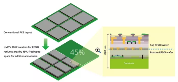
HSINCHU, Taiwan, May 2, 2024 — United Microelectronics Corporation (NYSE: UMC; TWSE: 2303) (“UMC”), a leading global semiconductor foundry, today announced the industry’s first 3D IC solution for RFSOI technology. Available on UMC’s 55nm RFSOI platform, the stacked silicon technology reduces die size by more than 45% without any degradation of radio frequency (RF) performance, enabling customers to efficiently integrate more RF components to address the greater bandwidth requirements of 5G.
As mobile device manufacturers pack more frequency bands in newer generations of smartphones, the company’s 3D IC solution for RFSOI addresses the challenge of integrating more RF front-end modules (RF-FEM) - critical components in devices to transmit and receive data – in a device by vertically stacking dies to reduce surface area. RFSOI is the foundry process used for RF chips such as low noise amplifiers, switches, and antenna tuners. Utilizing wafer-to-wafer bonding technology, UMC’s 3D IC solution for RFSOI resolves the common issue of RF interference between stacked dies. The company has received multiple patents for this process, which is now ready for production.
"We are proud to lead the industry in offering this state-of-the-art solution utilizing our innovative 3D IC technology for RF-FEM. This groundbreaking technology not only solves the challenges of increased frequency band demands in smartphones in the 5G/6G era, but also helps in mobile, IoT, and virtual reality devices with faster data transfer by accommodating more frequency bands in parallel,” said Raj Verma, Associate Vice President of Technology Development at UMC. “We are excited to continue developing stacked die solutions to meet our customers’ RF needs, such as for 5G millimeter-wave, in the future."
UMC offers the most comprehensive RF front-end module IC solutions in the industry, catering to a broad range of applications including mobile, Wi-Fi, automotive, IoT, and satellite communications. With over 500 product tape-outs completed and more than 38 billion RFSOI chips shipped, UMC’s family of RFSOI solutions are available in 8-inch and 12-inch wafers, as well as in a variety of technology nodes from 130nm to 40nm. In addition to RFSOI technologies, UMC’s 6-inch fab (Wavetek Microelectronics Corporation) offers compound semiconductor technologies gallium arsenide (GaAs) and gallium nitride (GaN) as well as RF filters to supplement the needs of RF-FEM applications.
About UMC
UMC (NYSE: UMC, TWSE: 2303) is a leading global semiconductor foundry company. The company provides high-quality IC fabrication services, focusing on logic and various specialty technologies to serve all major sectors of the electronics industry. UMC’s comprehensive IC processing technologies and manufacturing solutions include Logic/Mixed-Signal, embedded High-Voltage, embedded Non-Volatile-Memory, RFSOI, BCD etc. Most of UMC's 12-in and 8-in fabs with its core R&D are located in Taiwan, with additional ones throughout Asia. UMC has a total of 12 fabs in production with combined capacity of more than 400,000 wafers per month (12-in equivalent), and all of them are certified with IATF 16949 automotive quality standard. UMC is headquartered in Hsinchu, Taiwan, plus local offices in United States, Europe, China, Japan, Korea & Singapore, with a worldwide total of 20,000 employees. For more information, please visit: http://www.umc.com.
Related Chiplet
- Interconnect Chiplet
- 12nm EURYTION RFK1 - UCIe SP based Ka-Ku Band Chiplet Transceiver
- Bridglets
- Automotive AI Accelerator
- Direct Chiplet Interface
Related News
- UMC Launches W2W 3D IC Project with Partners, Targeting Growth in Edge AI
- TSMC Announces Breakthrough Set to Redefine the Future of 3D IC
- Siemens introduces Innovator3D IC - a comprehensive multiphysics cockpit for 3D IC design, verification and manufacturing
- Siemens and Intel Foundry advance their collaboration to enable cutting-edge integrated circuits and advanced packaging solutions for 2D and 3D IC
Latest News
- Where co-packaged optics (CPO) technology stands in 2026
- Qualcomm Completes Acquisition of Alphawave Semi
- Cadence Tapes Out UCIe IP Solution at 64G Speeds on TSMC N3P Technology
- Avnet ASIC and Bar-Ilan University Launch Innovation Center for Next Generation Chiplets
- SEMIFIVE Strengthens AI ASIC Market Position Through IPO “Targeting Global Markets with Advanced-nodes, Large-Die Designs, and 3D-IC Technologies”