TSMC plans automotive chiplet process for 2025
By Nick Flaherty, eeNews Europe (May 15, 2024)

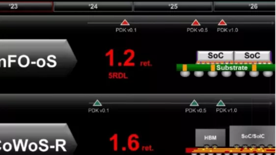
 TSMC is planning automotive qualified versions of its 3D fabric chiplet technology by the end of 2025.
The InFO-oS fanout technology will support multiple SoC devices on a substrate, with the first automotive chiplet process design kit (PDK) towards the end of this year and the full PDK early in 2026.
The CoWoS-R process will support SOCs with high performance HBM memory via an interposer to the substrate. The initial PDK will be available shortly with the full PDK similarly early in 2026.
To read the full article, click here
Related Chiplet
- DPIQ Tx PICs
- IMDD Tx PICs
- Near-Packaged Optics (NPO) Chiplet Solution
- High Performance Droplet
- Interconnect Chiplet
Related News
- Chiplet Pioneer Eliyan Achieves First Silicon in Record Time with Implementation in TSMC 5nm Process, Confirms Most Efficient Chiplet Interconnect Solution in the Multi-Die Era
- Renesas Unveils Industry’s First Automotive Multi-Domain SoC Built with 3-nm Process Technology with Chiplet Extensions
- TSMC drives A16, 3D process technology
- DreamBig Semiconductor Announces Partnership with Samsung Foundry to Launch Chiplets for World Leading MARS Chiplet Platform on 4nm FinFET Process Technology Featuring 3D HBM Integration to Solve Scale-up and Scale-out Limitations of AI for the Masses
Latest News
- LTSCT Joins imec Automotive Chiplet Program
- CEA-Leti Will Present Its Latest Advances On Next-Generation Chip Integration at ECTC 2026
- OpenLight Secures $50 Million in Series A-1 Funding to Accelerate Global Deployment of Next-Generation Photonics
- Lightmatter Names Roy Kim Vice President of Product to Lead Global Deployment of Photonic Interconnects
- Why Chip Sovereignty Is No Longer About Chips—But Systems