Report: SK Hynix mulls offering advance packaging foundry service
By Peter Clarke, eeNews Europe ( December 16, 2024)
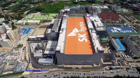
Memory chip vendor SK Hynix is considering a move into 2.5D chip packaging as a foundry outsource operation, according to South Korea’s ETnews.
The move may be partially driven by SK Hynix’s sub-ordinate role to foundry TSMC in the creation of AI accelerators for Nvidia. If SK Hynix could offer 2.5D packaging skills it could potentially offer to work in parallel with TSMC and perform the integration of GPU die and high-bandwidth memory (HBM) DRAM components in AI acceleration components.
To read the full article, click here
Related Chiplet
- Interconnect Chiplet
- 12nm EURYTION RFK1 - UCIe SP based Ka-Ku Band Chiplet Transceiver
- Bridglets
- Automotive AI Accelerator
- Direct Chiplet Interface
Related News
- SK hynix Signs Investment Agreement of Advanced Chip Packaging with Indiana
- SK hynix Signs Preliminary Memorandum of Terms with U.S. Department of Commerce for Advanced Packaging Facility in Indiana
- 2.5D/3D chip technology to advance semiconductor packaging
- JCET’s Automotive Chip Advanced Packaging Flagship Factory Project Gains Momentum
Latest News
- Where co-packaged optics (CPO) technology stands in 2026
- Qualcomm Completes Acquisition of Alphawave Semi
- Cadence Tapes Out UCIe IP Solution at 64G Speeds on TSMC N3P Technology
- Avnet ASIC and Bar-Ilan University Launch Innovation Center for Next Generation Chiplets
- SEMIFIVE Strengthens AI ASIC Market Position Through IPO “Targeting Global Markets with Advanced-nodes, Large-Die Designs, and 3D-IC Technologies”