2.5D/3D chip technology to advance semiconductor packaging
A team of researchers from the Institute of Science Tokyo (Science Tokyo), Japan, has conceptualised an innovative 2.5D/3D chip integration approach called BBCube.
By Jean-Pierre Joosting, eeNews Europe | June 23, 2025
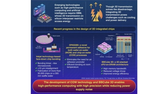
Traditional system-in-package (SiP) approaches, where semiconductor chips are arranged in a two-dimensional plane (2D) using solder bumps, have size-related limitations, warranting the development of novel chip integration technologies. For high-performance computing, the researchers developed a novel power supply technology by employing a 3D stacked computing architecture, which consists of processing units placed directly above stacks of dynamic random-access memory, marking a significant advance in 3D chip packaging.
To implement BBCube, the researchers developed key technologies involving precise and high-speed bonding techniques and adhesive technology. These new technologies can help address the demands of high-performance computing applications, which require both high memory bandwidth and low power consumption, with reduced power supply noise.
To read the full article, click here
Related Chiplet
- Interconnect Chiplet
- 12nm EURYTION RFK1 - UCIe SP based Ka-Ku Band Chiplet Transceiver
- Bridglets
- Automotive AI Accelerator
- Direct Chiplet Interface
Related News
- Amkor Technology Breaks Ground on New Semiconductor Advanced Packaging and Test Campus in Arizona; Expands Investment to $7 Billion
- PGC Integrates 2.5D/3D Advanced Packaging Technology to Break the “Memory Wall” and Accelerate AI/HPC ASIC Innovation
- BOS Joins VESA and UCIe to Advance Global Standards in Display and Chiplet Technology
- Resonac and PulseForge Unite to Advance Photonic Debonding for Next-Gen Semiconductor Packaging
Latest News
- Qualcomm Completes Acquisition of Alphawave Semi
- Cadence Tapes Out UCIe IP Solution at 64G Speeds on TSMC N3P Technology
- Avnet ASIC and Bar-Ilan University Launch Innovation Center for Next Generation Chiplets
- SEMIFIVE Strengthens AI ASIC Market Position Through IPO “Targeting Global Markets with Advanced-nodes, Large-Die Designs, and 3D-IC Technologies”
- FormFactor Expands Silicon Photonics Test Capabilities With Acquisition of Keystone Photonics