Niobium Superconducting Interconnects Open New Horizons for Quantum Computing
July 15, 2025 -- The development of quantum computers and their computational capabilities comes with a major challenge: increase more and more the number of quantum bits, or qubits—which in turn requires scaling up the number of interconnects in the integrated quantum systems. But how can this be achieved without disrupting the overall operation of the system? To address this challenge, research engineers at CEA-Leti have developed an innovative superconducting interconnect brick that could enable achieving a higher density of chip-to-chip connections while minimizing the thermal transfer between the chips.
The computing power of a quantum computer is closely linked to its number of qubits. To control and optimize their performance, 3D architectures are now being considered to connect qubit chips to other chips hosting control and readout circuits or devices. The resulting structure forms an integrated quantum system that can be placed directly into a cryostat and operated at just a few kelvins—or even millikelvins—depending on the type of qubit used.
Direct Bonding of Niobium Pads
So how can the number of qubits—and therefore the number of interconnects between different chips—be increased, while ensuring that qubits continue to operate at the required cryogenic temperatures, unaffected by the heat generated by other chips or system elements? That is the challenge that CEA-Leti's team, including Candice Thomas, a research engineer in 3D integration for quantum systems, is tackling.
“Our goal is to integrate superconducting materials into chip-to-chip interconnects because, at low temperatures, they conduct electrical signals perfectly, generate no heat—thanks to their zero resistance—and even help reduce heat transfer potentially generated by the control and readout circuits within the system, thanks to their poor thermal conductivity," she explains.
To implement these interconnects, the research team drew upon a technique in which CEA-Leti has recognized expertise: direct wafer-to-wafer bonding—a process where two surfaces are bonded without the use of adhesives. Typically used for other applications, mainly with copper, this method has now been adapted to a superconducting material: the niobium.
“We also removed the electrical insulator—specifically, the dielectric—normally found around copper pads, leaving only air around the interconnects, which should help reduce both thermal and radiofrequency losses in the system," says Thomas.
The resulting interconnects take the form of niobium pads, linking chips via this adapted direct bonding technique.
Connecting High-Density Qubit Arrays
Using this technique—a world first at this interconnect pitch—offers several advantages.
“Direct bonding will enable us to achieve very fine pitches, which is essential for scaling up qubit numbers and to support high-density signal architectures," notes Candice Thomas. “Moreover, our process only requires tools already used in the industry, which should facilitate technology transfer."
The team successfully produced a demonstrator with a 7 µm pitch, which allowed them to validate both the electrical and superconducting properties of the interconnects. Further testing is planned to evaluate their thermal performance and signal transmission characteristics. Researchers also aim to further reduce the interconnect pitch to meet the density requirements of silicon spin qubit systems.
Additionally, the team is working on optimizing the direct bonding process to make it compatible with the integration processes of various qubit technologies, especially superconducting qubits—advancements that could also benefit the broader field of superconducting electronics. This includes developing a chip-to-wafer bonding process and lowering the annealing temperature used to reconstruct the bonding interface.
“The process we're using today, inherited from hybrid Cu/SiO₂ bonding methods, requires an annealing at 400 °C, which could degrade the qubit performances, and even the superconducting properties of the materials forming the interconnects," says Candice Thomas. “We're now working on ways to reduce that annealing temperature."This would be a key step toward integrating this technological building block into future quantum system architectures.
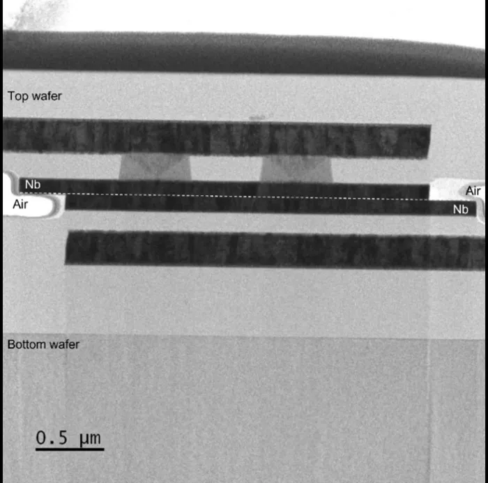
Figure 1 – Image obtained by scanning transmission electron microscopy showing the direct bonding of two Nb pads forming an interconnect between two wafers. The bonding interface between the two pads is highlighted with a white dashed line.
Related Chiplet
- Integrated voltage regulator (IVR) chiplet
- High-performance connectivity chiplets
- eFPGA Chiplet
- DPIQ Tx PICs
- IMDD Tx PICs
Related News
- What could back an open market for chiplets?
- Siluxtek and GlobalFoundries Forge a Deep Strategic Partnership to Mass-Produce 200G/Lane Silicon Photonic Receiver Chips, Paving the Way for the Industrial Revolution of AI Computing Interconnects
- JEDEC and Open Compute Project Foundation Pave the Way for a New Era of Chiplet Innovation
- EV Group and Fraunhofer IZM-ASSID Expand Partnership in Wafer Bonding for Quantum Computing Applications
Latest News
- Tessolve and Intel Foundry Collaborate on Enablement for EMIB Advanced Packaging Technology
- Intel and Lens Technology Collaborate to Enable Advanced Semiconductor Packaging for the AI Era
- Amkor Technology Announces Strategic Partnership with NVIDIA to Expand Advanced Packaging and Test for Next-Generation AI Infrastructure
- Synopsys Enables AMD Instinct™ MI455X GPU Design with Comprehensive Multi-Die Solution
- AI Data Centers Push Silicon Photonics Toward 300-mm Scale