NHanced Project Puts U.S. on Advanced-Packaging Map
EXCLUSIVE INTERVIEWS
By Alan Patterson, EETimes (January 26, 2024)
NHanced Semiconductors’ investment in hybrid bonding will make the company one of the first in the U.S. to offer advanced packaging services, the company president and experts told EE Times.
With its investment of several hundred million dollars, the company endeavors to put the U.S. back on the map in chip packaging, which today is primarily done in Asia. NHanced is aiming for the high end, using hybrid bonding to integrate chip dies with interconnect pitches in the range of 10 microns.
“When it comes to hybrid bonding of heterogeneous material, we are the only commercial supplier in the world,” NHanced President Bob Patti told EE Times. “We have probably a good three-year head start on anyone.”
NHanced will be among the first companies in the U.S. to do hybrid bonding, TechSearch President Jan Vardaman told EE Times.
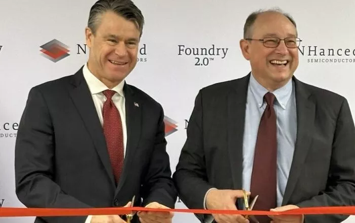
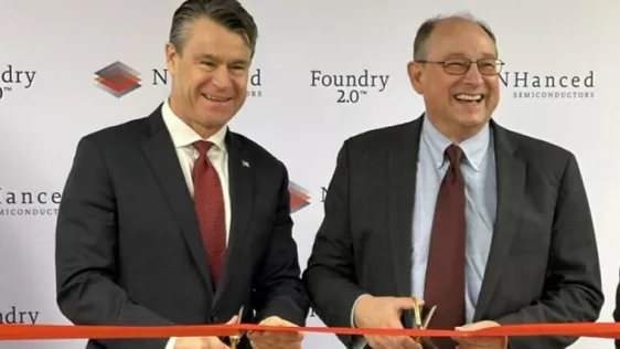
U.S. Sen. Todd Young (R-Ind.), left, joined Nhanced CEO Bob Patti at the opening of an advanced packaging facility this month. (Source: NHanced)
“There is a shortage of silicon interposers and assembly for that because of the surprise demand from Nvidia’s AI play,” she said. “There are some companies in the U.S. that need a U.S. source of silicon interposers, and NHanced should be able to provide this.”
To read the full article, click here
Related Chiplet
- DPIQ Tx PICs
- IMDD Tx PICs
- Near-Packaged Optics (NPO) Chiplet Solution
- High Performance Droplet
- Interconnect Chiplet
Related News
- GlobalFoundries and U.S. Department of Commerce Announce Award Agreement on CHIPS Act Funding for Essential Chip Manufacturing
- ASU and Deca Technologies selected to lead $100M SHIELD USA project to strengthen U.S. semiconductor packaging capabilities
- STARLight Project chosen as the European consortium to take the lead in next-generation Silicon Photonics on 300mm wafers
- Eliyan Sets New Standard for Chiplet Interconnect Performance with Latest PHY Delivering Data Rate of 64Gbps on 3nm Process Using Standard Packaging
Latest News
- Agileo Automation Launches Agil'EDA to Accelerate SEMI EDA Adoption for Semiconductor Equipment OEMs
- AEM and ASE Enter Strategic Partnership to Accelerate AI and HPC Test Innovation
- NLM Photonics Samples Silicon Organic Hybrid PICs Manufactured at GlobalFoundries
- Avalanche Technology and NHanced Semiconductors Leverage Advanced 2.5D Integration to Bring Optimal SWaP and Reliability to Rad-Hard FPGAs
- Open EU Foundry status granted to innovative chiplet facility