The Evolution of Interconnects in Microelectronics Packaging
By Dr. Dongkai Shangguan
3DIncites (November 14, 2024)
Semiconductor packaging is a complex and evolving field, involving multiple disciplines. As a microelectronics packaging engineer, I focus on the “interconnect thread” from the chip to the system (Figure 1).
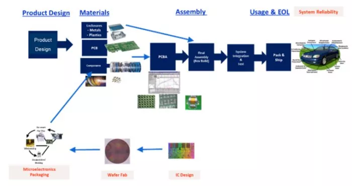
To me, packaging is about interconnectivity (essentially). The primary function of packaging is to provide the interconnection from the IC to the system, for signal distribution and power distribution. What makes it more complex (and thus interesting) is the enabling functions, including mechanical reliability (especially under complex loading conditions in diverse use environments – thus various failure modes and mechanisms); thermal dissipation (especially important for high power and also due to the multiple interfaces in the system); as well as manufacturability that has to be considered (such as low temperature soldering, fine pitch processes, cost and quality, and very importantly, sustainability). These electro-mechano-thermal functions of the interconnect are what makes “packaging” such a critical area for semiconductor technology today. In the age of heterogeneous integration, a variety of interconnects in the same package have to be considered.
To read the full article, click here
Related Chiplet
- DPIQ Tx PICs
- IMDD Tx PICs
- Near-Packaged Optics (NPO) Chiplet Solution
- High Performance Droplet
- Interconnect Chiplet
Related News
- 2024 IEEE Electronic Components and Technology Conference to Spotlight Cutting-Edge Microelectronics Packaging Technologies; Photonic Devices, Heterogeneous Integration are Among Key Topics
- How do UCIe and BoW interconnects support generative AI on chiplets?
- How can in-package optical interconnects enhance chiplet generative AI performance?
- How does UCIe on chiplets enable optical interconnects in data centers?
Latest News
- Ultra Accelerator Link™ (UALink™) Consortium Publishes Four Specifications Defining In-Network Compute, Chiplets, Manageability and 200G Performance
- CEA-Leti, CEA-List and PSMC Collaborate to Integrate RISC-V and MicroLED Silicon Photonics into 3D Stacking and Interposer for Next-Generation AI
- NIST Researchers Develop Photonic Chip Packaging That Can Withstand Extreme Environments
- Rebellions Closes $400 Million Pre-IPO and Launches RebelRack™ and RebelPOD™ to Accelerate Global Expansion
- EdgeCortix Looks To Chiplets For Third-Gen Reconfigurable AI Chip