Intel’s Expanding IP Portfolio in Co-Packaged Optics
SOPHIA ANTIPOLIS, France – November 13, 2025 – As demand for data-intensive computing continues to rise, Intel has developed an extensive suite of patents addressing the integration of photonic and electronic systems at the package level. These inventions collectively illustrate the transition from traditional electrical interconnects toward optical input/output (I/O) architectures that enable higher bandwidth, lower latency, and improved energy efficiency across compute and networking platforms. This article focuses on Intel’s strategy and key innovations in co-packaged optics (CPO) and optical interconnects (optical I/O), ahead of our upcoming advanced packaging intellectual property (IP) landscape report that will provide an overview of the patent activity and strategies of the key players in this field.
A patent-powered shift: Intel’s road to co-packaged optics and optical I/O
At the 2024 Optical Fiber Communication conference, Intel’s Integrated Photonics Solutions group unveiled a prototype Optical Compute Interconnect (OCI) chiplet, a fully integrated optical I/O device co-packaged with a CPU and transmitting live data. Demonstrating 4 Tb/s of bidirectional throughput at approximately 5 pJ/bit, the prototype underscored Intel’s progress toward scalable, energy-efficient optical interconnects designed to meet the extreme bandwidth and power demands of AI infrastructure and high-performance data centers. Although still at the prototype stage, the OCI marked a decisive step toward unifying photonics and electronics within a single computing package, a convergence widely regarded as essential for overcoming the limitations of copper-based interconnects. By moving optical I/O closer to the processor, Intel aims to reduce latency, power consumption, and signal loss while dramatically increasing interconnect density, a foundational advance for future heterogeneous computing systems.
Intel’s live demonstration provides a tangible glimpse into its long-term vision: the transition from pluggable optical transceivers toward tightly co-packaged, light-based interconnects. This shift reflects broader trends across the semiconductor industry, where the integration of optical components directly into compute packages is seen as a path to sustained performance scaling. The OCI prototype therefore serves not just as a proof of concept, but as a technological marker for Intel’s broader roadmap, one that blends advances in silicon photonics, advanced packaging, and thermal co-design to redefine how data moves within and between compute systems.
A patent landscape of integrated photonics innovation
Beneath public communications lies an extensive and evolving patent portfolio that maps Intel’s strategic progress in photonic-electronic integration. These patents reveal a systematic effort to merge optics, electronics, packaging, and thermal management across multiple levels of integration, from on-package optical I/O and co-packaged opto-electronic assemblies to emerging glass interposers and embedded cooling architectures. Viewed collectively, these inventions trace Intel’s trajectory from early optical interconnect research toward a comprehensive platform strategy that unites photonics and silicon computing. They illustrate a clear shift away from discrete optical modules toward dense, light-enabled interconnect fabrics that could transform system-level performance, efficiency, and scalability.
Over the past five years, the semiconductor company has shown a strong upward trend in patenting activity. Its robust and expanding IP portfolio reflects a dynamic innovation pipeline, with numerous pending applications filed across major markets, particularly the US, Europe, and China (figure 1).
This technological and intellectual property evolution highlights how Intel is positioning itself at the forefront of the next computing paradigm; one where light is not merely a transmission medium, but an integral component of data processing itself.
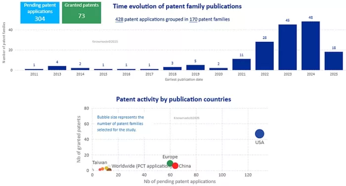
Figure 1: Time evolution of patent family publications and geographical distribution of granted patents and pending applications from Intel for co-packaged optics and optical interconnects. Note: The data corresponding to the year 2025 is not complete since the patent search was done in June 2025.
1. Co-packaged opto-electronics: Vertical integration at the system level
Intel addresses data center networking challenges in patent US11217573 (figure 2), which describes a network switching package optimized for high-bandwidth photonic integration. The patent proposes stacking photonic engines (320) on both the top and bottom surfaces of the package substrate (305), thereby doubling available bandwidth without expanding the footprint. Sockets with extended stand-off heights create space below the interposer for thermal management and optical coupling, minimizing signal loss and improving power efficiency. This vertically integrated structure enables scalable bandwidth density for next-generation network switches, achieving higher total throughput within the same footprint.
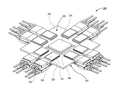
Figure 2: Stacked photonic engines in network switching package (Intel, US11217573).
2. Co-packaged opto-electronics: Optical I/O at the processor level
The patent US9507086 (figure 3) details one of Intel’s foundational approaches to on-package optical integration. Here, lasers, modulators, photodetectors, and couplers are mounted directly onto the processor substrate, enabling optical signals to communicate with the processor without intermediate electrical conversions. This reduces latency, increases aggregate bandwidth, and improves energy-per-bit performance, all while maintaining compatibility with existing CMOS fabrication and packaging methods. This patent establishes Intel’s early and continuing leadership in bringing optical interconnects directly onto processor packages, transforming compute fabrics for AI and cloud-scale workloads.
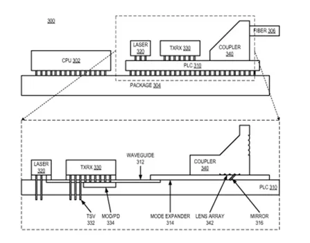
Figure 3: Processor-level optical integration with on-package lasers and modulators, for electrical free I/O (Intel, US9507086).
Patent US12266608 (figure 4, left) introduces a co-packaged design that directly integrates a heterogeneous processing unit (XPU) with a photonic integrated circuit (PIC) using Intel’s Embedded Multi-die Interconnect Bridge (EMIB). The design employs fan-out redistribution layers (FORDL) to electrically couple the XPU and PIC through the EMIB, extending signal reach without performance degradation. This arrangement supports optical I/O within a single package, delivering ultra-high bandwidth over optical links, beyond the limits of electrical traces. The approach combines compact packaging and scalable optical interconnects, enabling efficient on-package photonics for HPC and data center applications.
Expanding on this concept, the patent application US20230090863 (figure 4, right) presents an optical fanout interposer architecture aimed at directly coupling XPUs with PICs through integrated waveguides (120–122). These waveguides form an “optical interposer” layer that connects logic and photonic dies with minimal electrical path length. The design supports bandwidths exceeding one petabyte per second through dense passive optical routing, while passive alignment of components simplifies manufacturing and improves yield. The resulting structure achieves extremely high data density and low-latency photonic communication, representing a major step toward disaggregated compute architectures interconnected by light.
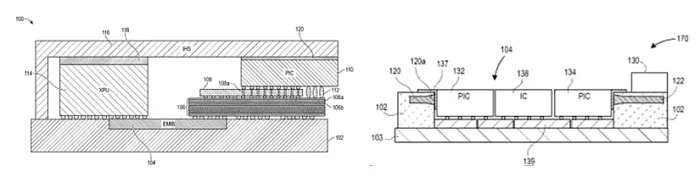
Figure 4: Left – EMIB-based co-packaged XPU–PIC integration (Intel, US12266608); Right – Optical fanout interposer with embedded waveguides (Intel, US20230090863).
3. Glass substrates: Toward optical interposers
To meet interconnect density and integration requirements beyond the limits of silicon, Intel has pioneered the use of glass substrates and hybrid bonding as the foundation for scalable opto-electronic packaging. These approaches offer improved planarity, reduced loss, and greater dimensional stability for complex optical-electrical assemblies.
Patent application US20240178207 (figure 5) introduces a glass-core interposer (103) incorporating through-glass vias (TGVs 110) that transmit both electrical and optical signals. Waveguides embedded within the glass allow for high-bandwidth optical transmission, while TGVs provide fine-pitch electrical connectivity (2–70 µm). By hybrid bonding a photonic integrated circuit to the glass substrate, optically through one portion of its active surface and electrically through another, the design achieves tight optical alignment and high interconnect density in a compact footprint. This architecture bridges the gap between traditional electrical interposers and optical interconnect layers, offering an elegant path toward glass-based optical interposers for scalable data communication modules.
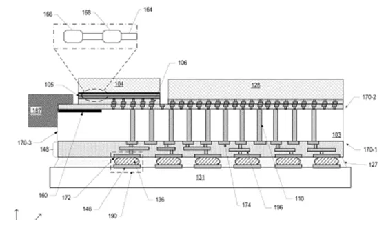
Figure 5: Glass-core interposer with through-glass vias (Intel, US20240178207).
Similarly, the patent US12147083 describes a hybrid manufacturing process where electronic and photonic structures are bonded into a unified microelectronic assembly. The approach allows ICs containing optical elements (waveguides, modulators, or lenses) to be bonded with electronic dies containing transistors or interconnects, forming a heterogeneous stack. Additional photonic or electronic features, such as conductive vias or dielectric waveguides, can be fabricated post-bonding to enhance performance. This flexibility allows seamless photonic-electronic integration and scalability across different process technologies. In application US20230093438, Intel extends glass-based packaging to PIC-to-PIC optical communication. Photonic dies are mounted onto a glass substrate containing passive glass waveguides that provide low-loss optical links between disaggregated dies or off-package components. The architecture supports high signaling frequencies and long-reach optical channels with minimal loss, enabling direct optical communication across multi-die systems.
Combined, these patents underscore Intel’s transition from silicon interposers to glass-based, hybrid-bonded photonic platforms, a key enabler for future exascale computing and disaggregated chiplet architectures.
4. Integrated thermal management in photonic–electronic packaging
As co-packaged optics evolve toward higher power densities and denser integration, thermal management has emerged as one of the most critical challenges to reliable operation. Intel’s patents in this area reveal a multi-faceted strategy that integrates heat spreading, power delivery, and mechanical support directly into the package architecture.
Patent application US20220413236 (figure 6, left) introduces a thermally conductive, electrically active “thermal die” (330) positioned above the photonic integrated circuit (308). This thermal die provides a dual function: delivering electrical power from the substrate to the PIC while simultaneously extracting heat from localized hot spots, especially from on-chip lasers. The heat is transferred to an integrated heat spreader (324), eliminating the need for TSVs or wire bonds and simplifying assembly. This multifunctional structure enhances power delivery efficiency, thermal performance, and reliability while maintaining a compact form factor suitable for co-packaged optical engines.
Complementary to this, US20250110301 (figure 6, right) tackles the thermal bottlenecks that occur when a PIC is placed between an electronic integrated circuit and the package lid. The patent application introduces thermal plugs embedded within the PIC’s dielectric layers that connect high-heat regions directly to the substrate. These high-conductivity plugs efficiently transfer heat from both the PIC (204) and adjacent EIC dies (202, 208, 206), maintaining temperature uniformity and operational stability under heavy load. The arrangement minimizes thermal gradients and ensures reliable long-term performance for high-speed optical-electronic modules.
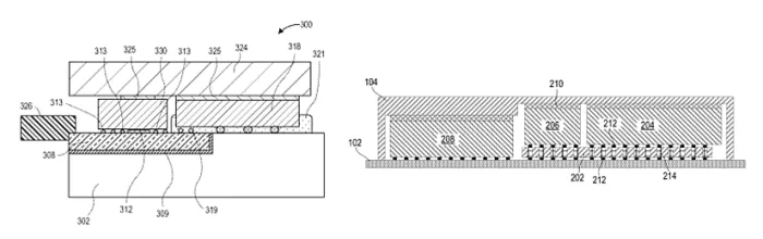
Figure 6: Thermal die and plug-based cooling for PIC/EIC packages (Intel, US20220413236, left image; Intel, US20250110301, right image).
Through these innovations, Intel addresses the intertwined issues of thermal and electrical co-design in optical packaging. The introduction of integrated thermal dies and embedded thermal plugs reflects a holistic strategy that links cooling, power, and packaging, a necessary step toward practical, large-scale deployment of co-packaged optical systems.
Conclusion
Intel’s patent portfolio reveals a unified strategy to merge photonics and electronics across every level of system design. From vertically integrated network packages that increase bandwidth density without increasing footprint, to processor-level optical I/O, glass-based interposers, and integrated thermal solutions, these innovations collectively redefine how data, power, and heat are managed within high-performance systems. The progression reflects a decisive shift away from discrete optical modules toward compact, light-enabled interconnect fabrics that deliver exceptional bandwidth efficiency and scalability. Together, these advances illustrate Intel’s drive to establish photonic–electronic integration as the cornerstone of next-generation AI, cloud, and data-center computing.
While Intel’s innovations clearly position the company as a leading force in the transition toward photonic-electronic integration, it is far from alone in shaping this technological revolution. Other key IP players are also investing heavily in co-packaged optics and optical interconnect technologies. Our forthcoming advanced packaging IP landscape report on CPO & Optical I/O will examine their patent portfolios and strategies, offering a comprehensive view of the competitive ecosystem driving the next generation of optical connectivity.
About the author
Pauline Calka, PhD. works for KnowMade as a patent analyst in the fields of semiconductor manufacturing and advanced packaging. She holds a PhD in Memory from the University of Grenoble Alpes (France), in partnership with the CEA-Leti (France). After an Alexander von Humboldt Postdoc fellowship position at the Technical University of Berlin (Germany) and the Leibniz Institute for High Performance Microelectronics on ReRAM development, Pauline worked five years at ASM International (Belgium) as Senior Process Engineer on thin film development for logic, memory and MEMS, and two years at CEA-Leti as Integration Engineer on imaging CMOS sensors.
About KnowMade
KnowMade is a technology intelligence and IP strategy consulting company specialized in analyzing patents and scientific publications. The company helps innovative companies, investors, and R&D organizations to understand competitive landscape, follow technological evolutions, reduce uncertainties, and identify opportunities and risks in terms of technology and intellectual property.
KnowMade’s analysts combine their strong technology expertise and in-depth knowledge of patents with powerful analytics tools and methodologies to turn patent information and scientific literature into actionable insights, providing high added value reports for decision makers working in R&D, innovation strategy, intellectual property, and marketing. Our experts provide prior art search, patent landscape analysis, freedom-to-operate analysis, IP due diligence, and monitoring services.
KnowMade has a solid expertise in Compound Semiconductors, Power Electronics, Batteries, RF Technologies & Wireless Communications, Solid-State Lighting & Display, Photonics, Memories, MEMS & Sensors, Semiconductor Packaging, Medical Devices, Medical Imaging, Microfluidics, Biotechnology, Pharmaceutics, and Agri-Food.
Related Chiplet
- DPIQ Tx PICs
- IMDD Tx PICs
- Near-Packaged Optics (NPO) Chiplet Solution
- High Performance Droplet
- Interconnect Chiplet
Related News
- Omni Design Technologies Advances 200G-Class Co-Packaged Optics IP Portfolio for Next-Generation AI Infrastructure
- Co-packaged Optics and Optical Interconnects: A Global Picture of the IP Competition
- Lightmatter Collaborates with Synopsys to Integrate Advanced Interface IP with Its Passage Co-Packaged Optics Platform
- RANOVUS delivers industry’s first 6.4Tbps Co-Packaged Optics with integrated laser for AI/ML application at OFC 2024
Latest News
- NIST Researchers Develop Photonic Chip Packaging That Can Withstand Extreme Environments
- Rebellions Closes $400 Million Pre-IPO and Launches RebelRack™ and RebelPOD™ to Accelerate Global Expansion
- EdgeCortix Looks To Chiplets For Third-Gen Reconfigurable AI Chip
- Agileo Automation Launches Agil'EDA to Accelerate SEMI EDA Adoption for Semiconductor Equipment OEMs
- AEM and ASE Enter Strategic Partnership to Accelerate AI and HPC Test Innovation