CEA Combines 3D Integration Technologies & Many-Core Architectures to Enable High-Performance Processors That Will Power Exascale Computing
SAN FRANCISCO – Dec. 15, 2020 – CEA-List and CEA-Leti, research institutes at CEA, presented their technologies for achieving exascale-level, high- performance computing (HPC). Highlighting CEA-List’s advanced demonstrators and CEA-Leti’s state-of-the-art, 3D-technology toolbox that together enable higher bandwidth and heterogeneity for processors, the researchers explain how these empowered properties are critical for hardware innovations that help enable exascale computing.
Exascale computing refers to computing systems capable of calculating at least 10¹⁸, or one-billion-billion, floating-point operations per second, which would be twice as fast as the fastest computer available today. Efforts to develop exascale computing are driven by highly data-intensive scientific and industrial applications, such as climate research, drug discovery and material design. This level of performance in HPC and Big Data will be achieved with heterogeneous computing nodes composed of generic processor chiplets hosting accelerator chiplets for improved operational intensity.
“Profound evolutions brought by high performance computing (HPC) applications are based on continuous and exponential increases in computing performances over the past decades,” explained Denis Dutoit, a CEA-List scientist and lead author of the IEDM paper, How 3D integration technologies enable advanced compute node for Exascale-level High Performance Computing?. “Supercomputers will soon achieve exascale-level computing performances mainly thanks to the introduction of innovative hardware technologies around the processors.”

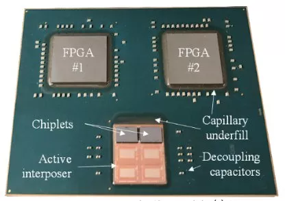
ExaNoDe Heterogeneous Multi-Chip Module (c) CEA
The CEA technologies are powering demonstrators in the ExaNoDe and INTACT projects, which have developed integrated prototypes with technology building blocks to support the EU’s drive towards exascale computing. The two institutes combined expertise in silicon and 3D sequential integration with many-core architectures, which are differentiated by their high level of scalability and power efficiency. They have demonstrated the benefit of new integration methods and processes following two main paths: finer 3D interconnect pitches, leading to improved bandwidth between compute chiplets, and assembly technologies that allow increasing heterogeneity in packaging, which improves peak performance.
In addition, the importance of a 3D-integration solution to developing HPC processors is confirmed by the European Processor Initiative (EPI), with which CEA is deeply involved. Its aim is to design and implement a roadmap for a new family of low-power European processors for extreme scale computing, high-performance Big Data and a range of emerging applications.
“These R&D successes open a path towards heterogeneous processors that will enable exascale-level supercomputers,” said Denis Dutoit. “We demonstrated that co-optimization of advanced architectures with 3D integration technologies achieves the level of computing performance and bandwidth required for HPC.”
Because chiplets stacked on active interposer allow modularity and reusability at low development costs, CEA-List also is investigating using this new methodology for HPC architectures in the embedded world, for compute-intensive accelerators. For edge applications requiring a high level of computation and memory, such as artificial intelligence (AI), chiplet-based partitioning will enable the creation of a broad range of solutions to meet the needs for embedded AI. Potential uses include autonomous driving, transport applications and industry 4.0.
Current CEA-Leti research work addresses die-to-wafer direct hybrid-bonding technology, which offers denser 3D interconnects with better electrical, mechanical and thermal parameters, and allows ultrahigh-bandwidth capabilities in heterogeneous systems. CEA-Leti also is working on high-density through silicon vias (TSV) (pitch 1 to 4 µms) to create together with die-to-wafer hybrid bonding a complete dense 3D stack. For the longer term, CEA-Leti is also investigating innovative photonic-interposer technology as a 3D-based photonic chiplet approach to enable interconnection of tens of computing chiplets with the resulting chip-to-chip communication bandwidth, latency and energy.
Over the next decade, co-optimization of advanced integration technologies with disruptive architectures is expected to establish the key foundations for HPC components.
This work was funded by the French National Programme d’Investissements d’Avenir (Investments in the Future), IRT Nanoelec, under Grant ANR-10-AIRT-05.
This work also was supported by the ExaNoDe project, funded by the European Union’s H2020 program under grant agreement No. 671578.
Related Chiplet
- DPIQ Tx PICs
- IMDD Tx PICs
- Near-Packaged Optics (NPO) Chiplet Solution
- High Performance Droplet
- Interconnect Chiplet
Related News
- CEA-Leti & STMicroelectronics’ Paper at IEDM 2025 Demonstrates Path to Fully Monolithic Silicon RF Front-Ends with 3D Sequential Integration
- Veeco and imec develop 300mm compatible process to enable integration of barium titanate on silicon photonics
- CEA-Leti, CEA-List and PSMC Collaborate to Integrate RISC-V and MicroLED Silicon Photonics into 3D Stacking and Interposer for Next-Generation AI
- Synopsys Collaborates with TSMC to Enable 2D and 3D Design Solutions
Latest News
- Ultra Accelerator Link™ (UALink™) Consortium Publishes Four Specifications Defining In-Network Compute, Chiplets, Manageability and 200G Performance
- CEA-Leti, CEA-List and PSMC Collaborate to Integrate RISC-V and MicroLED Silicon Photonics into 3D Stacking and Interposer for Next-Generation AI
- NIST Researchers Develop Photonic Chip Packaging That Can Withstand Extreme Environments
- Rebellions Closes $400 Million Pre-IPO and Launches RebelRack™ and RebelPOD™ to Accelerate Global Expansion
- EdgeCortix Looks To Chiplets For Third-Gen Reconfigurable AI Chip