Bringing Tiny Chiplets To Embedded SoCs
By Sally Ward-Foxton, EETimes (October 31, 2023)
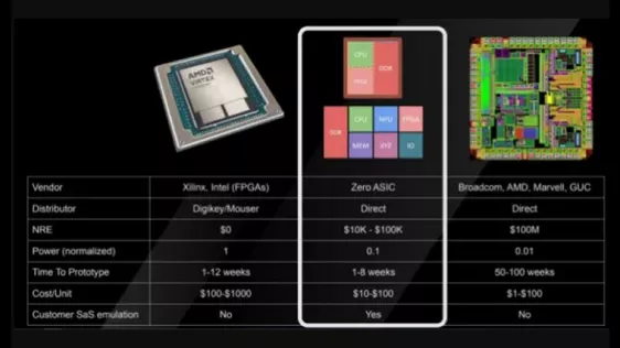
LONDON — ZeroASIC has developed a technology platform to bring chiplets to embedded system design, as a time-efficient alternative to designing and manufacturing custom application-specific ICs (ASICs). The platform is based on swappable pre-fabbed 2 x 2 mm chiplets on an active silicon interposer, which customers can design for themselves in a matter of minutes using ZeroASIC’s online EDA tool.
The company’s aim is to reduce the barrier to making custom ASICs versus using off-the-shelf SoCs. ZeroASIC CEO Andreas Olofsson told EE Times that the biggest cost, in terms of both time and money, for custom ASICs is tapeouts.
To read the full article, click here
Related Chiplet
- Interconnect Chiplet
- 12nm EURYTION RFK1 - UCIe SP based Ka-Ku Band Chiplet Transceiver
- Bridglets
- Automotive AI Accelerator
- Direct Chiplet Interface
Related News
- Empower Semiconductor Showcases High-Density Power Chiplets and Embedded Integrated Voltage Regulators at APEC 2024
- Baya Systems Introduces New Technology to Transform SoCs and Chiplets for Emerging Applications
- On chip voltage regulator IP for chiplets and SoCs
- Alphawave Semi to Reveal Ecosystem and Key Architectures Unlocking Generative AI Potential at EE Times' "Chiplets: Building the Future of SoCs" Seminar
Latest News
- Qualcomm Completes Acquisition of Alphawave Semi
- Cadence Tapes Out UCIe IP Solution at 64G Speeds on TSMC N3P Technology
- Avnet ASIC and Bar-Ilan University Launch Innovation Center for Next Generation Chiplets
- SEMIFIVE Strengthens AI ASIC Market Position Through IPO “Targeting Global Markets with Advanced-nodes, Large-Die Designs, and 3D-IC Technologies”
- FormFactor Expands Silicon Photonics Test Capabilities With Acquisition of Keystone Photonics