YMTC’s Hybrid Bonding Patents: A Key Competitive Factor for Memory Chipmakers
By Pauline Calka, Patent Analyst, KnowMade
SOPHIA ANTIPOLIS, France – June 19, 2025 – Hybrid bonding is a technique that connects two semiconductor chips by directly bonding copper interconnects to copper and insulating materials to insulating materials. Unlike conventional chip-stacking methods that rely on solder balls or bumps, hybrid bonding enables thinner packaging while improving both electrical and thermal performance.
Over the past five years, hybrid bonding technology has emerged as a key enabler of advanced semiconductor packaging. Driven by the aggressive R&D efforts of global semiconductor companies, the number of hybrid bonding-related patents has increased more than fourfold since 2019, accompanied by a significant transformation of the competitive intellectual property (IP) landscape. In our latest Hybrid Bonding Patent Landscape report, we identified TSMC, Adeia, and Yangtze Memory Technologies Corp (YMTC) as leading players in hybrid bonding IP.
Hybrid bonding technology has a wide range of applications. In the memory sector, it is expected to be implemented in next-generation high-bandwidth memory (HBM) with more than 20 stacked layers, 3D DRAM, and NAND flash with over 400 layers. In fact, hybrid bonding has already been commercialized in the NAND market. Chinese chipmaker YMTC has been mass-producing NAND chips using this technology, marketed as “Xtacking”, for about four years. This process involves wafer-to-wafer (W2W) bonding, where the core components of NAND (the cell and peripheral circuits) are fabricated separately on different wafers and then bonded together.
YMTC’s patent portfolio is particularly noteworthy. An analysis of 25 of the company’s key patents reveals that the company possesses advanced technologies related to 3D memory architectures involving NAND, DRAM, and SRAM; hybrid bonding of logic and memory dies; and the integration of peripheral circuits around bonding layers. YMTC’s patents enable heterogeneous stacking of logic, memory, and controllers, enhancing the viability of semiconductor manufacturing for artificial intelligence (AI) and high-performance computing (HPC) applications. Additionally, the company holds a broad range of patents related to manufacturing processes, including surface treatments, barrier layer engineering, precise alignment methods, stress compensation, and wafer dicing techniques required for implementing hybrid bonding.
The Hybrid Bonding Patent Landscape Is Dynamic, With Evolving IP Leaders and the Entry of New Patent Applicants
Patent analytics reveal a surge in patent publications related to advanced semiconductor packaging worldwide. Among the key technologies, hybrid bonding has shown the most significant acceleration in patent filings. In our recent IP report, we selected and analyzed more than 5,800 patents published globally, representing over 1,600 patent families (groups of patent applications filed in multiple countries to protect a single invention).
As pioneer, Adeia (formerly Xperi) acquired the direct bond interconnect (DBI®) technology from Ziptronix in 2015 and has been licensing it to various companies, including Sony, YMTC, Micron, and Kioxia, ever since. Despite Adeia’s historically strong IP position, other players have been developing their own patent portfolios related to hybrid bonding processes or die stacking using hybrid bonding technology. TSMC and Intel have invested in R&D efforts from the early days in this cutting-edge bonding technology, developing their own IP portfolios and advanced packaging innovations for chiplets, such as TSMC’s 3D-stacked System-on-Integrated Chips (SoIC) and Intel’s Foveros Direct. After DBI® technology entered the image sensor market in 2016 through Sony’s CMOS image sensor in Samsung’s Galaxy S7, memory makers like Micron, Samsung, and YMTC joined the IP race. Beyond memory applications, hybrid bonding has become essential for achieving the most advanced packaging capabilities. Consequently, China is investing heavily in this technology, with YMTC and XMC increasing their hybrid bonding-related patenting activities, while TongFu Mircroelectronics, SJSemi, and CXMT have entered the hybrid bonding IP landscape over the last years.
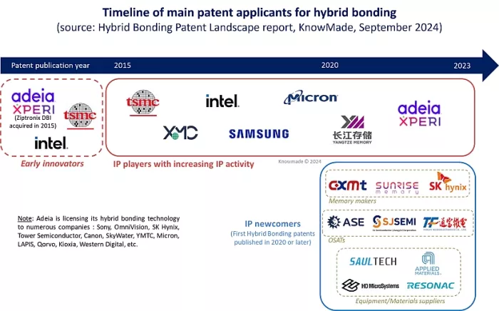
Figure 1: Main patents assignees for hybrid bonding technology and their entry into the patent landscape (Source: Hybrid Bonding Patent Landscape report, KnowMade, September 2024)
TSMC leads the hybrid bonding patent landscape from a quantitative viewpoint, with most of its inventions related to hybrid-bonded semiconductor structures or devices, primarily focused on 2.5D and 3D IC applications. YMTC and Adeia have significantly expanded their enforceable patent portfolios in recent years. Adeia holds the largest number of key patents related to the bonding process itself, and its IP portfolio encompasses a wide range of innovations aimed at improving the reliability of hybrid bonding structures, such as thermal management, mechanical stress reduction, metal diffusion control, and bonding strength. YMTC’s hybrid bonding patents are particularly notable for their focus on 3D-stacked memory technologies. While foundries and device makers dominated the IP race prior to 2020, OSATs and equipment/material suppliers have recently entered the hybrid bonding patent landscape with rapidly growing portfolios. Companies such as ASE, SJSemi, TongFu, Applied Materials, and Resonac are now emerging as new IP challengers.
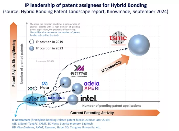
Figure 2: Number of granted patents and pending patent applications held by main patent assignees for hybrid bonding technology (Source: Hybrid Bonding Patent Landscape report, KnowMade, September 2024)
YMTC’s Hybrid Bonding-Related Patents as a Major Factor for Memory Manufacturers
YMTC was the first company to apply hybrid bonding technology to 3D NAND chips in 2018-2019, introducing it under the name “Xtacking”. The company initially acquired foundational patents from Xperi (now Adeia) through a licensing agreement during the early stages of its business. Since then, YMTC has developed and expanded its own patent portfolio.
YMTC’s strong position in hybrid bonding patents is putting pressure on South Korean memory giants Samsung Electronics and SK Hynix. According to a report by ZDNet Korea, Samsung has reportedly set to license hybrid bonding patents from YMTC to manufacture its next-generation NAND flash chips. SK Hynix is also expected to pursue a similar agreement. This move underscores the difficulty of circumventing YMTC’s patents, which are viewed as unavoidable. The decision to obtain a license rather than challenge the patents legally suggests that the South Korean firms are prioritizing technological progress over IP disputes.
YMTC’s IP activity is outpacing South Korean leaders in this domain. Between 2017 and January 2024, YMTC disclosed 119 hybrid bonding-related patents. In contrast, Samsung Electronics, despite beginning publications as early as 2015, had only disclosed 83 patents by the end of 2023. SK Hynix, which began filing patent later, had disclosed just 11.
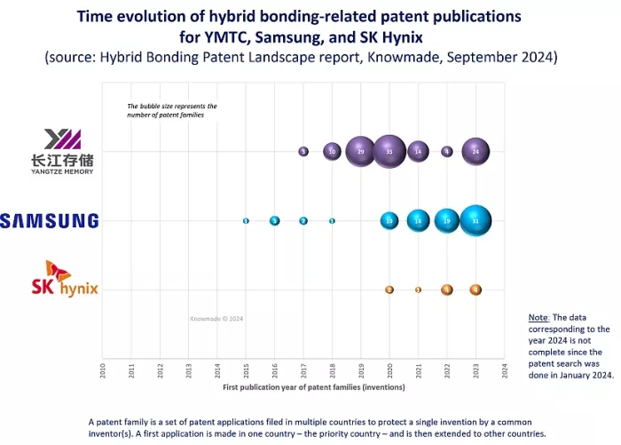
Figure 3: Time evolution of patent publications related to hybrid bonding technology for YMTC, Samsung, and SK Hynix (Source: Hybrid Bonding Patent Landscape report, KnowMade, September 2024)
YMTC’s Strategic Patent Portfolio for Hybrid Bonding Technology
Patents related to hybrid bonding can be categorized into three main types of claimed inventions:
- Semiconductor structures or devices utilizing hybrid bonding interconnects,
- Hybrid bonding manufacturing processes and interface engineering, and
- Equipment used for hybrid bonding.
While most patents focus on hybrid-bonded structures and devices, the hybrid bonding process itself has recently attracted significant IP interest from key industry players. The top three IP players Adeia, TSMC, and YMTC, are the leading patent assignees in this area. Their innovations are primarily aimed at improving process reliability, including stress management, bonding strength, and bonding structure alignment. This focus reflects ongoing R&D efforts to further advance hybrid bonding technology.
Among the 1,600 hybrid bonding-related patent families, Knowmade has identified over 280 key patented inventions that are most critical in terms of prior art, IP risks, and technology. The main patent assignees TSMC, Adeia, Intel, YMTC and Samsung own key hybrid bonding-related patents on both bonding process and bonded semiconductor structure or device.
25 key patent families have been identified for YMTC. These innovations aim at pushing the limits of memory density, performance, and integration through three-dimensional (3D) stacking enabled by hybrid bonding. The company’s key patents are systematically addressing the bottlenecks of planar architecture, such as scaling, cost, and integration limitations, by introducing vertically integrated device structures. YMTC key hybrid bonding-related patents reflect a convergence of advanced 3D memory architectures (NAND, DRAM, SRAM), innovative hybrid bonding techniques, heterogeneous integration of logic and memory, and manufacturing process optimizations.
YMTC’s key patents for hybrid bonding
Most YMTC’s key patents propose new 3D memory device designs involving vertically stacked NAND, DRAM, and SRAM arrays (e.g., patent applications WO2020/211332 and WO2020/232573), separated logic and memory dies integrated through hybrid bonding (WO2020/220593, WO2021/163944), and peripheral circuits distributed across multiple bonded layers (WO2023/272555, WO2023/272614, WO2023/272627). These architectures overcome 2D scaling limits by reducing substrate area, enabling multi-functional stacking (logic + memory + control), and facilitating heterogeneous integration for AI and HPC applications.
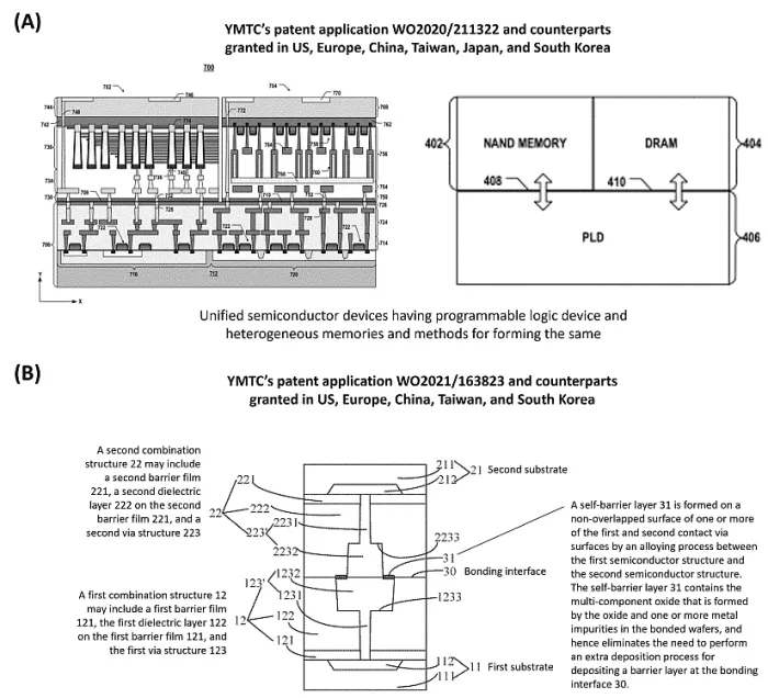
Figure 4: Example of YMTC’s key patents (A) WO2020/211322 and (B) WO2021/163823
The hybrid bonding technical foundation (die-to-die or wafer-to-wafer) allows face-to-face, face-to-back, and back-to-back interconnects, precise alignment of contacts with both functional and dummy VIAs (WO2020/154939, WO2020/154954), and enhanced reliability and electrical performance via novel bonding layers and barrier materials (WO2021/163823, WO2021/138792).
Several key inventions describe vertical memory cells with vertical gate transistors to maximize density (WO2023/028829, WO2023/028869), mirror-symmetric layouts for structural and routing efficiency (WO2023/028869), and novel interconnect architectures for back-side pad-outs (WO2022/047649).
YMTC holds also key patents related to fabrication processes, enabling ion-implanted buried stop layers for precise substrate thinning (WO2022/204959), self-aligned diffusion barriers to avoid metal diffusion issues during bonding (WO2021/163823), and modular separation of the capacitor array wafer and periphery transistor wafers, including the array transistors of the DRAM, to decouple process steps and improve manufacturing yield (WO2021/163944).
YMTC’s patent related to hybrid bonding manufacturing methods
YMTC holds more than 20 patent families related to manufacturing methods involving hybrid bonding techniques, most of which have been filed only in China.
Several patents propose novel surface treatments (e.g., plasma activation WO2020/140212), bonding of dissimilar materials (e.g., metal-dielectric bonding WO2021/138792), and barrier layer engineering (e.g., graphene barriers CN109148417, CN107993928) to enhance bonding strength, reliability, and interface quality. Other inventions address stress-induced defects during bonding through stress balancing (CN107731668) and continuous pressure annealing (CN107993927), aiming to improve alignment accuracy and reduce dislocation risks. Precise wafer dicing methods crucial for hybrid bonding are proposed (e.g., plasma-based methods CN114226984, slag-free cutting CN113953689, and advanced trenching WO2023/197665), addressing flatness, slag, and structural damage issues.
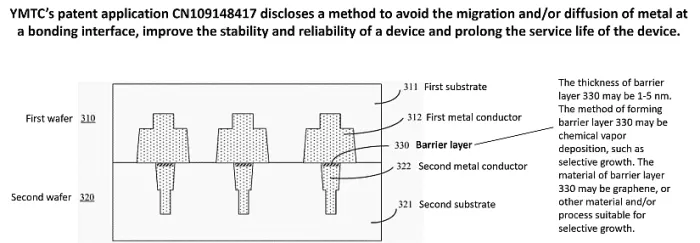
Figure 5: Example of YMTC’s patent related to hybrid bonding manufacturing methods (CN109148417).
Hybrid bonding enables YMTC to overcome planar scaling bottlenecks by creating dense vertical interconnects (WO2020/154939, WO2020/103025). Patents propose high-density, low-footprint designs tailored for future memory and logic devices.
The bonding interface is a recurring technical battleground. Copper diffusion and electromigration are mitigated via graphene capping (CN107993928) and planar graphene barriers (CN109148417). Alloyed oxides at the interface provide a self-aligning diffusion block (WO2021/163823). Metal-dielectric bonding overcomes traditional bonding defects (WO2021/138792).
Maintaining precise alignment during bonding is critical, and some YMTC’s patents focus on precise alignment feedback to minimize misalignment defects. The CN108511419 introduces test capacitors to monitor misalignment in real time, and the CN110783234 proposes laser-based measurements to dynamically adjust wafer positions.
Several patents aim to reduce process complexity and photomask counts. Single-sided vertical interconnect access (VIA) structures (CN111162041) eliminate the need for dual-sided VIA etching, and dual-purpose bonding/interconnect layers (CN107731667) streamline metal usage.
Some patents relate to stress compensation and bow correction, such as temporary photoresist plus backside tensile film to control wafer bow during bonding (CN107731668), or continuous pressure during annealing to strengthen bonds (CN107993927).
Eventually, CN114226984 (plasma-enhanced multi-stage cutting), CN113953689 (Pre-removal of metal pads before dicing to reduce slag), and WO2023/197665 (precision cutting of hybrid bonded wafers for sub-µm features) represent a focused effort on improving dicing methods to preserve surface flatness and minimize damage.
Hybrid bonding, as an enabler of high-density 3D integration, is central, addressing both performance and manufacturability. Breaking down logic, memory, and peripheral circuits into separate dies maximizes process flexibility and yields. YMTC’s patent portfolio reflects a cohesive, innovation-led strategy focused on unlocking the next generation of memory and logic integration through advanced 3D architectures enabled by hybrid bonding. The company is not only solving near-term scaling problems but also laying a foundation for future, high-performance memory systems suitable for AI and HPC. The vertical integration of programmable logic and high-speed memory targets high-throughput applications. Innovations such as buried stop layers and pad-out schemes demonstrate attention to real-world production constraints. Architectures are designed to accommodate increased stack height, finer features, and future-generation memory technologies. Each patent contributes to a modular, scalable, and manufacturable platform that leverages vertical stacking to deliver breakthroughs in density, efficiency, and system-level integration.
Stay Ahead in Advanced Semiconductor Packaging with KnowMade’s Patent Intelligence Solutions
At KnowMade, we specialize in transforming patent data into actionable insights to support strategic decision-making in R&D, innovation, intellectual property, and investment. Throughout the year, we continuously track and analyze the latest patenting activities of competitors involved in advanced semiconductor packaging. Our analysis reports, monitoring services, and consultancy provide unique and valuable insights into cutting-edge innovations and the evolving technological and competitive landscape.
For a deeper and more comprehensive view of hybrid bonding, including competitive intelligence, technology developments, and IP strategies, we invite you to explore our Hybrid Bonding Patent Landscape report. Subscribing to our Advanced Packaging Patent Monitor allows you to gain timely insights into advanced semiconductor packaging, including Fan-Out, 2.5D & 3D IC, hybrid bonding, chiplets, and co-packaged optics. For a tailored study adapted to your specific needs, feel free to contact us at contact@knowmade.fr
About the author
Pauline Calka, PhD. works for KnowMade as a patent analyst in the fields of semiconductor manufacturing and advanced packaging. She holds a PhD in Memory from the University of Grenoble Alpes (France), in partnership with the CEA-Leti (France). After an Alexander von Humboldt Postdoc fellowship position at the Technical University of Berlin (Germany) and the Leibniz Institute for High Performance Microelectronics on ReRAM development, Pauline worked five years at ASM International (Belgium) as Senior Process Engineer on thin film development for logic, memory and MEMS, and two years at CEA-Leti as Integration Engineer on imaging CMOS sensors.
Nicolas Baron, PhD. is the CEO and co-founder of KnowMade. He manages the development and strategic orientation of the company and personally leads the semiconductor department. He holds a PhD in Physics from the University of Nice Sophia-Antipolis, and a Master of Intellectual Property Strategies and Innovation from the European Institute for Enterprise and Intellectual Property (IEEPI), Strasbourg, France.
About KnowMade
KnowMade is a technology intelligence and IP strategy consulting company specialized in analyzing patents and scientific publications. The company helps innovative companies, investors, and R&D organizations to understand competitive landscape, follow technological evolutions, reduce uncertainties, and identify opportunities and risks in terms of technology and intellectual property.
KnowMade’s analysts combine their strong technology expertise and in-depth knowledge of patents with powerful analytics tools and methodologies to turn patent information and scientific literature into actionable insights, providing high added value reports for decision makers working in R&D, innovation strategy, intellectual property, and marketing. Our experts provide prior art search, patent landscape analysis, freedom-to-operate analysis, IP due diligence, and monitoring services.
KnowMade has a solid expertise in Compound Semiconductors, Power Electronics, Batteries, RF Technologies & Wireless Communications, Solid-State Lighting & Display, Photonics, Memories, MEMS & Sensors, Semiconductor Packaging, Medical Devices, Medical Imaging, Microfluidics, Biotechnology, Pharmaceutics, and Agri-Food.
Related Chiplet
- eFPGA Chiplet
- DPIQ Tx PICs
- IMDD Tx PICs
- Near-Packaged Optics (NPO) Chiplet Solution
- High Performance Droplet
Related News
- Adeia Demonstrates Hybrid Bonding Technology During Chiplet Summit 2024
- Adeia Presents Metrology Techniques for Improved Yield in Hybrid Bonding at IMAPS Device Packaging Conference 2024
- SEMI 3D & Systems Summit to Spotlight Trends in Hybrid Bonding, Chiplet Design and Environmental Sustainability
- EV Group Hybrid Bonding, Maskless Lithography and Layer Transfer Solutions for Heterogeneous Integration to be Highlighted at ECTC 2024
Latest News
- Allegro DVT Plays a Pivotal Role in Groundbreaking CHASSIS Automotive Base Die Development
- CEO Interview: Rebellions’ NPU Leverages Memory-Centric Chiplets
- Applied Materials Introduces New Systems to Accelerate DRAM and Advanced Packaging for AI Chips
- Quantum Computing Inc. Completes Acquisition of NHanced Semiconductors, Inc.
- GlobalFoundries qualifies SLATE™ advanced packaging technology on 9SW platform for next-generation radio frequency applications