HBM5 20hi Stack to Adopt Hybrid Bonding Technology, Potentially Transforming Business Models
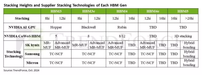
October 30, 2024 -- TrendForce reports that the focus on HBM products in the DRAM industry is increasingly turning attention toward advanced packaging technologies like hybrid bonding. Major HBM manufacturers are considering whether to adopt hybrid bonding for HBM4 16hi stack products but have confirmed plans to implement this technology in the HBM5 20hi stack generation.
Hybrid bonding offers several advantages when compared to the more widely used micro-bumping. Since it does not require bumps, it allows for more stacked layers and can accommodate thicker chips that help address warpage. Hybrid-bonded chips also benefit from faster data transmission and improved heat dissipation.
TrendForce indicates that the three major manufacturers will continue to use Advanced MR-MUF and TC-NCF stacking architectures for the HBM3e 12hi stack and HBM4 12hi stack. Meanwhile, a clear preference for the HBM4 16hi stack and HBM4e 16hi stack has yet to emerge between hybrid bonding and micro-bumping as hybrid bonding currently lacks significant advantages over micro-bumping.
If manufacturers opt for hybrid bonding, it would likely be to master the learning curve of this new stacking technology early to ensure smoother mass production of HBM4e and HBM5 products in the future. Manufacturers have confirmed that hybrid bonding will be used in the HBM5 20hi stack generation after taking into consideration limitations on stack height, IO density, and thermal management.
However, hybrid bonding comes with several challenges. For instance, manufacturers investing in new equipment to introduce the technology would reduce their reliance on micro-bumping, thereby losing any accumulated advantages in that area.
Hybrid bonding also presents technical challenges—such as particle control—which could drive up unit investment costs. Additionally, hybrid bonding requires wafer-to-wafer stacking, which could lead to inefficiencies if front-end production yields are too low and make overall production economically unfeasible.
TrendForce notes that the adoption of hybrid bonding could lead to significant shifts in the HBM business model. It becomes critical to ensure that the base die and memory die have identical chip dimensions with wafer-to-wafer stacking. Since the design of the base die is primarily handled by GPU/ASIC companies, TSMC, which offers both base die and GPU/ASIC foundry services, could take on the responsibility of stacking the base die and memory die. Should this development occur, it could significantly impact HBM manufacturers’ role in base die design, stacking, and overall HBM order management—potentially reshaping the competitive landscape.

For more information on reports and market data from TrendForce’s Department of Semiconductor Research, please click here, or email the Sales Department at SR_MI@trendforce.com
For additional insights from TrendForce analysts on the latest tech industry news, trends, and forecasts, please visit https://www.trendforce.com/news/
Related Chiplet
- DPIQ Tx PICs
- IMDD Tx PICs
- Near-Packaged Optics (NPO) Chiplet Solution
- High Performance Droplet
- Interconnect Chiplet
Related News
- Adeia Demonstrates Hybrid Bonding Technology During Chiplet Summit 2024
- Adeia Presents Metrology Techniques for Improved Yield in Hybrid Bonding at IMAPS Device Packaging Conference 2024
- SEMI 3D & Systems Summit to Spotlight Trends in Hybrid Bonding, Chiplet Design and Environmental Sustainability
- EV Group Hybrid Bonding, Maskless Lithography and Layer Transfer Solutions for Heterogeneous Integration to be Highlighted at ECTC 2024
Latest News
- NLM Photonics Samples Silicon Organic Hybrid PICs Manufactured at GlobalFoundries
- Avalanche Technology and NHanced Semiconductors Leverage Advanced 2.5D Integration to Bring Optimal SWaP and Reliability to Rad-Hard FPGAs
- Open EU Foundry status granted to innovative chiplet facility
- Siluxtek and GlobalFoundries Forge a Deep Strategic Partnership to Mass-Produce 200G/Lane Silicon Photonic Receiver Chips, Paving the Way for the Industrial Revolution of AI Computing Interconnects
- Lightwave Logic High-Speed Modulator Platform Now Available in GDS Factory PDK for GlobalFoundries Silicon Photonics Platform