Advanced IC Packaging: The Roadmap to 3D IC Semiconductor Scaling
I recently had the privilege of sitting down with Jan Vardaman, President of TechSearch International and a leading authority in semiconductor packaging analysis, to discuss the transformative shifts occurring in integrated circuit design and manufacturing. “Our focus is entirely on advanced packaging, and the developments we’re seeing now are happening faster than ever,” Vardaman explained, setting the stage for an informative discussion about the semiconductor industry’s evolution toward chiplet-based architectures.
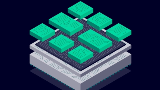
As the semiconductor industry approaches a projected market value of $1 trillion by 2030, the transition from traditional monolithic architectures to modular chiplet-based designs represents a fundamental shift in integrated circuit development. During our conversation, Vardaman provided crucial insights into why this transition is occurring: “The reason we’re seeing so much interest in the idea of the chiplet is that it offers a new way to design an IC. We can no longer afford to fabricate everything as a monolithic die on the most expensive nodes.”
To read the full article, click here
Related Chiplet
- Interconnect Chiplet
- 12nm EURYTION RFK1 - UCIe SP based Ka-Ku Band Chiplet Transceiver
- Bridglets
- Automotive AI Accelerator
- Direct Chiplet Interface
Related News
- KLA Unveils Comprehensive IC Substrate Portfolio for a New Era of Advanced Semiconductor Packaging
- Siemens and Intel Foundry advance their collaboration to enable cutting-edge integrated circuits and advanced packaging solutions for 2D and 3D IC
- “From Lab to Fab” – Innovative front-end and advanced packaging technologies for the semiconductor value chain
- nepes corporation expands IC packaging capabilities for the 3DIC era with advanced design flows from Siemens
Latest News
- Cadence Launches Partner Ecosystem to Accelerate Chiplet Time to Market
- Ambiq and Bravechip Cut Smart Ring Costs by 85% with New Edge AI Chiplet
- TI accelerates the shift toward autonomous vehicles with expanded automotive portfolio
- Where co-packaged optics (CPO) technology stands in 2026
- Qualcomm Completes Acquisition of Alphawave Semi