Using a Simulation Model to Optimize UCIe Implementations

By Hee-Soo Lee, High-Speed Design Lead, Keysight Technologies; Adrian Auge, Sr Staff Signal Integrity Engineer, Alphawave Semi; Fangyi Rao, Master R&D Engineer, Keysight Technologies

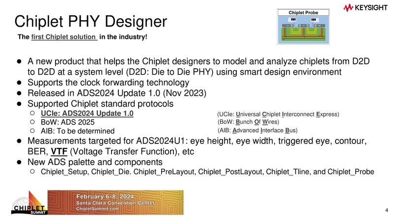
UCIe has become a popular standard for interconnecting dies within a package. A simulation model is essential for optimizing implementations. For example, a new tool, Chiplet PHY Designer, generates an electrical simulation model for die-to-die (D2D) PHY IP. A demonstration project takes the foundational aspects of the UCI electrical interface and uses them to generate a model based on the tool. It thus provides a practical example of how the electrical performance of a D2D link can be captured through simulation. The simulation allows designers to optimize UCIe implementations and take full advantage of the technology.

Introduction
Agenda
Introduction to Chiplet PHY Designer
Chiplet PHY Designer
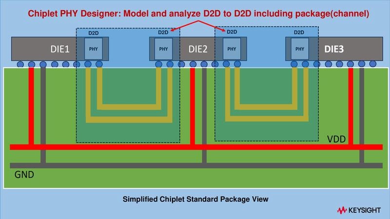
Model and analyze D2D to D2D including package(channel)
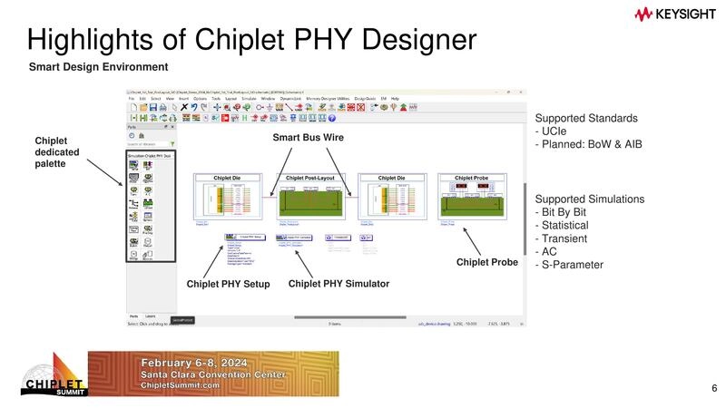
Highlights of Chiplet PHY Designer
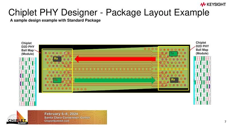
Package Layout Example
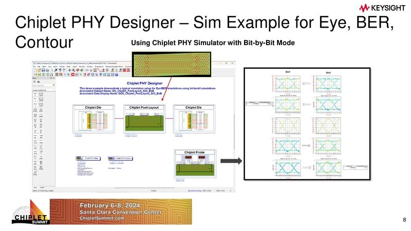
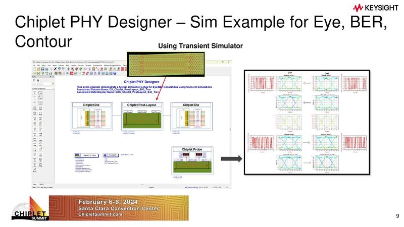
Sim Example for Eye, BER,  Contour 
Sim Example for Eye, BER, Contour
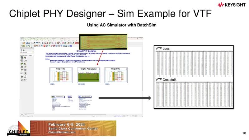
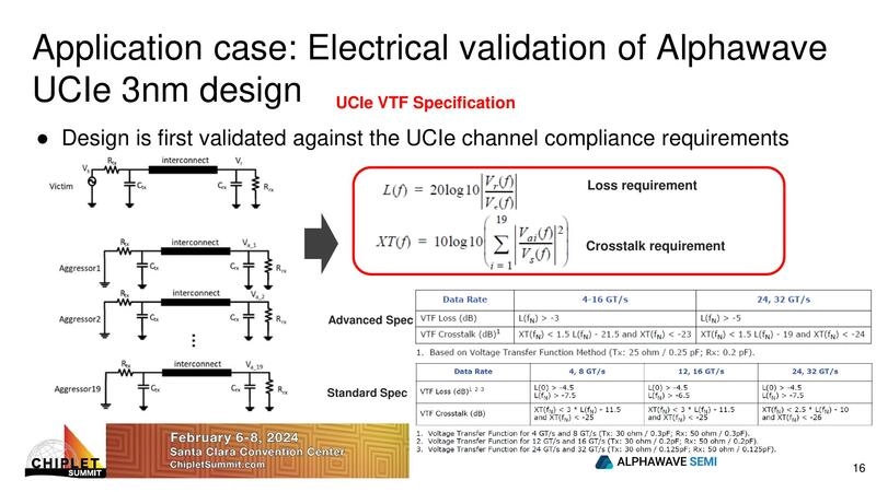
Sim Example for VTF
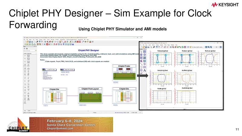
Sim Example for Clock Forwarding
Application Cases
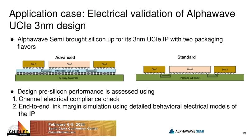
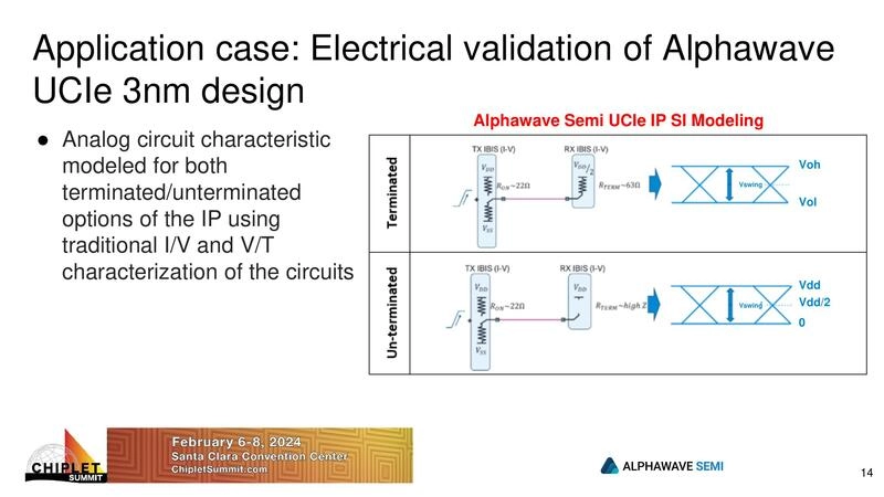
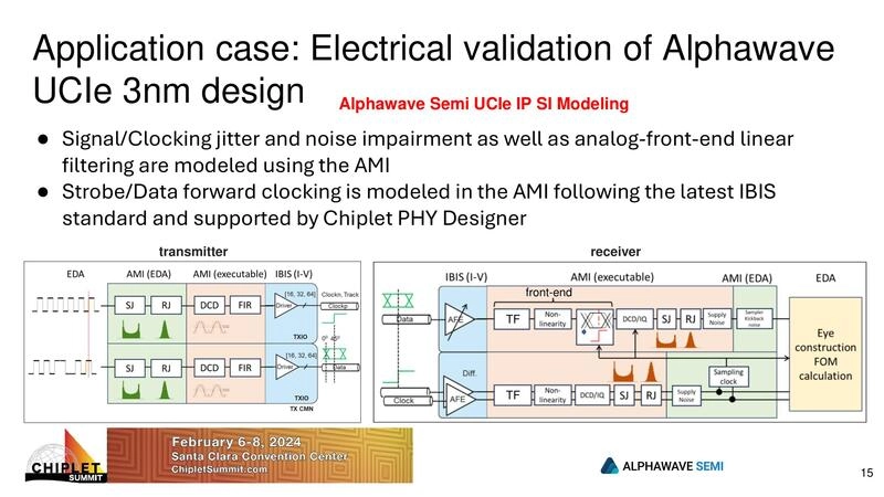
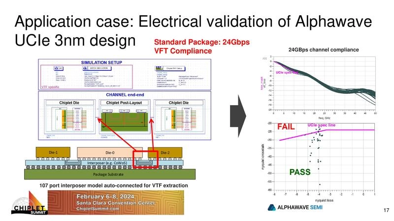
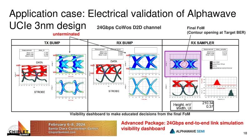
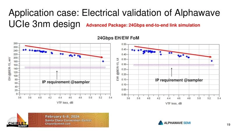
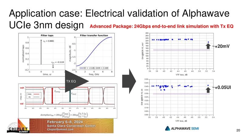
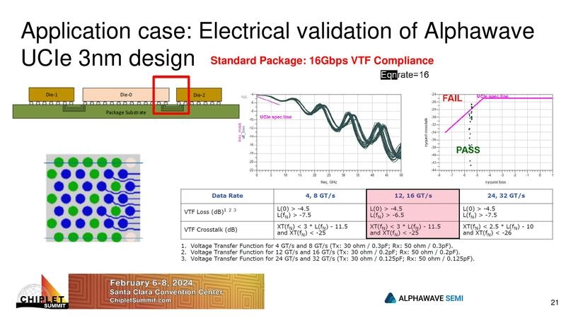
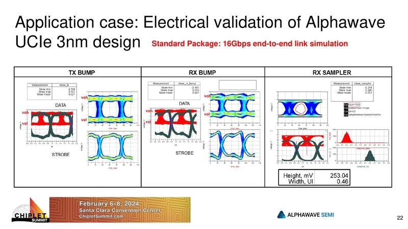
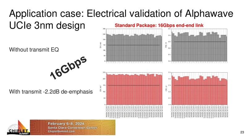
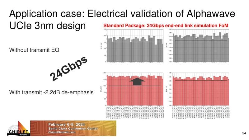
Electrical validation of Alphawave UCIe 3nm design
Summary