Protecting Against ESD in Die-to-Die Interfaces
By Bart Keppens, Chief Business Development, Sofics
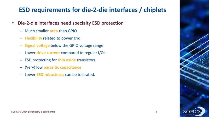
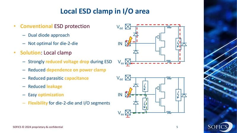
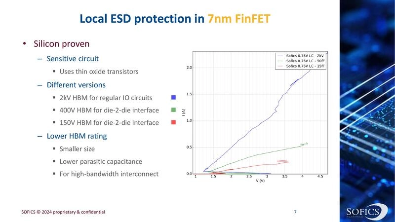
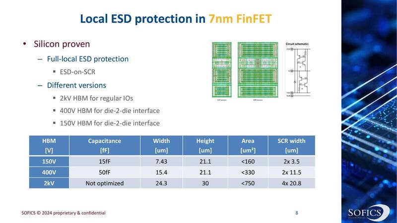
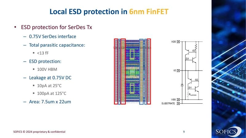
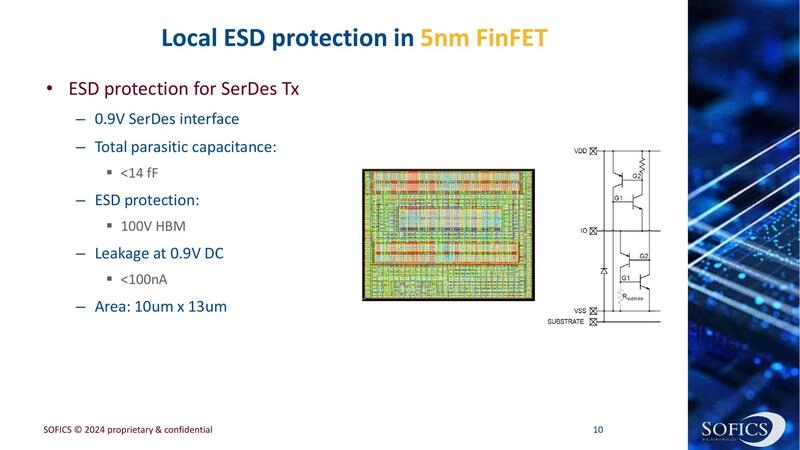
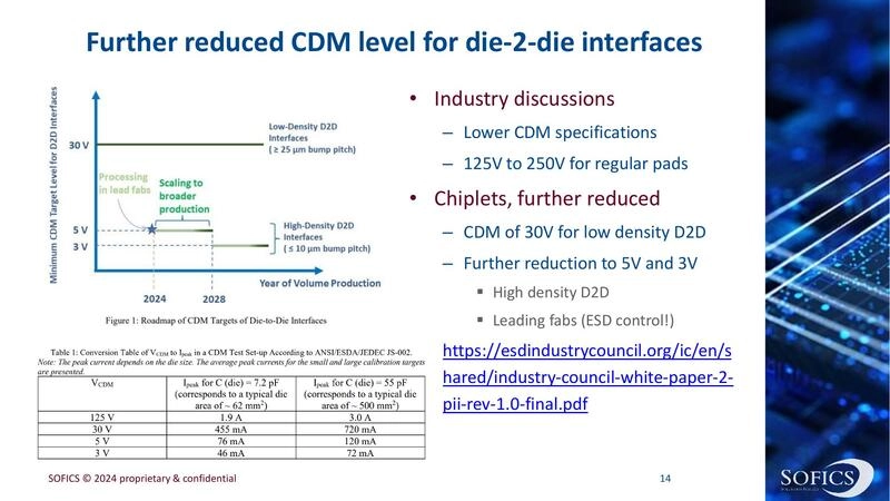
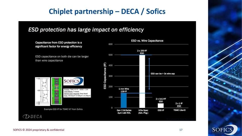
Designers sometimes drop electrostatic discharge (ESD) protection clamps completely for die-to-die interfaces. Once sealed in the package, nothing can touch the pads so danger is unlikely. However, experts recommend some ESD protection to ensure the chiplet assembly process has enough yield. How much is enough? Industry experts recently settled on standards and robustness levels for chiplets. However, some designers still prefer to reduce robustness levels to allow smaller ESD diodes. This approach could cause problems as the interfaces use sensitive thin oxide transistors. Recent discussions focus on ESD events relevant to chiplets, industry proposals for ESD protection, and example solutions used in several applications. Special die-to-die ESD solutions have been used on a wide range of TSMC technologies.
