By Rita Horner, Sr Director Product Marketing, Synopsys
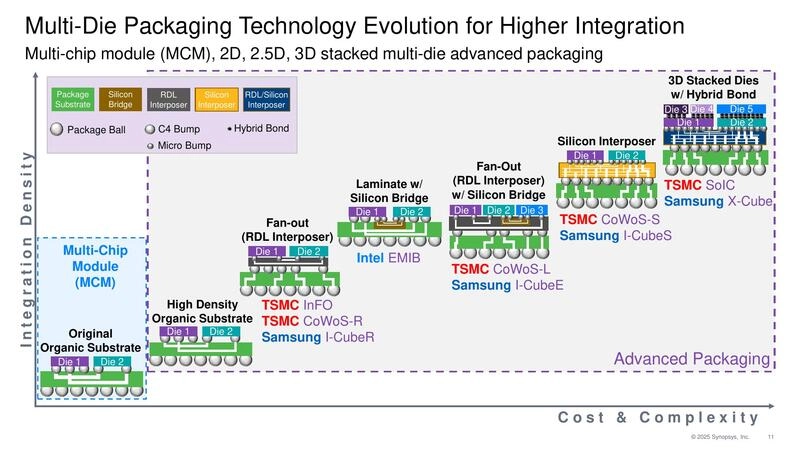
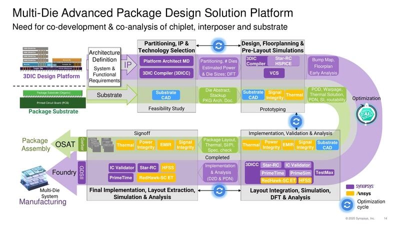
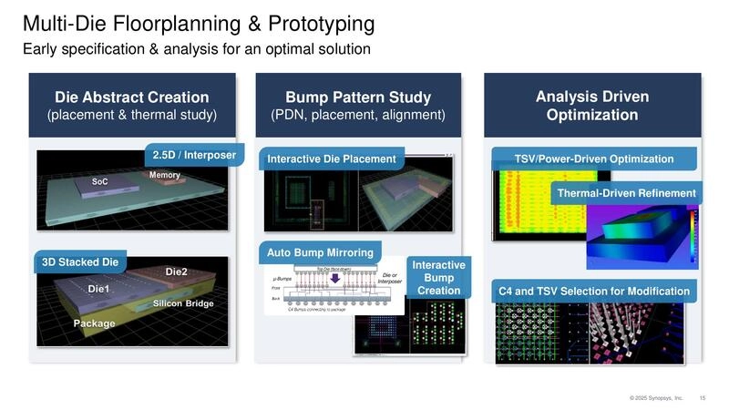
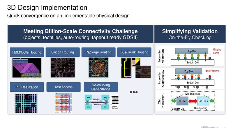
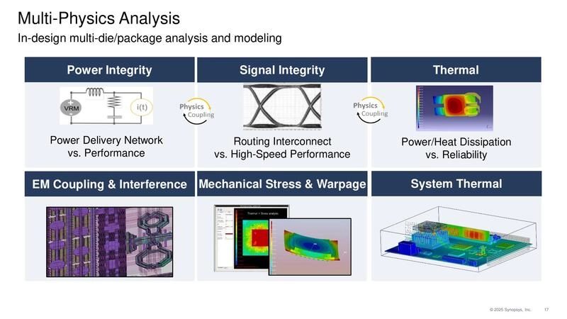
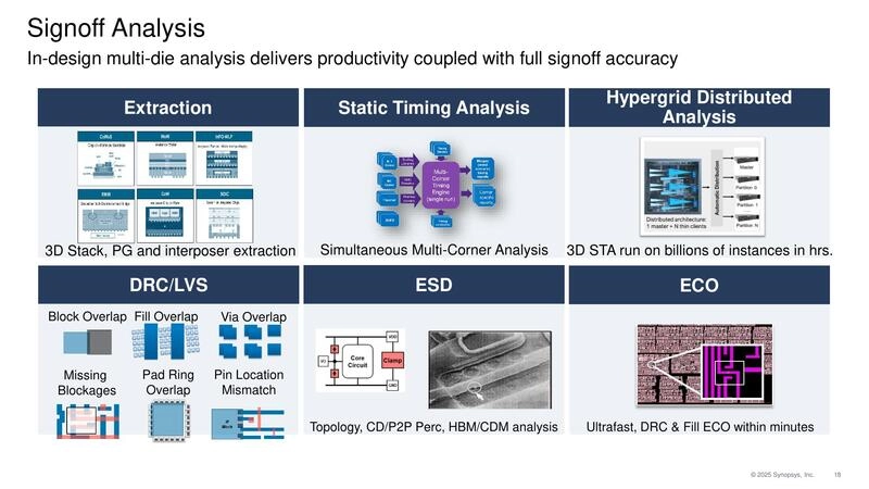
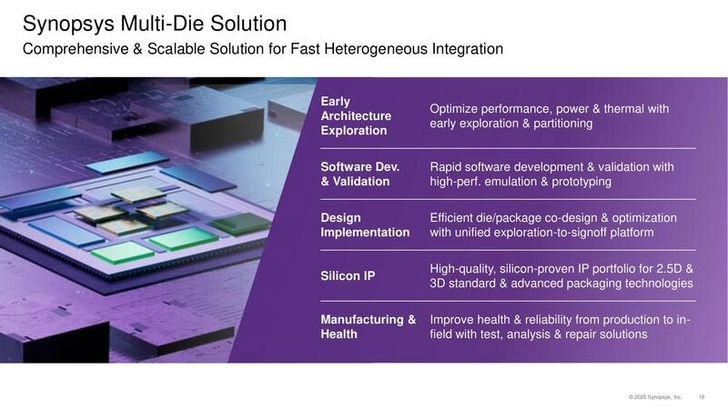
Multi-die design has become commonplace in many applications such as high-performance computing, networking, automotive, and mobile. Since multi-die designs involve multiple chiplets, designers must have both a chiplet-level and a system-level view at all times. A typical design example shows how this works. The process starts with early architecture exploration which benefits greatly from the bridging of functional and physical architectures. It continues to design implementation with thermal, signal and power integrity analysis occurring at both chiplet and system-level. Finally, signoff includes the integration of the chiplets and the analysis of the full design so it is ready for testing and manufacturing.