Known Good Die Enables Advanced Packaging & Chiplet Manufacturing
By Pat Pisano, Sr. Director Test Strategy, Intel Foundry
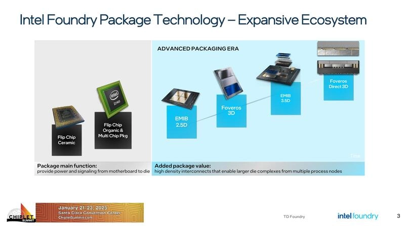
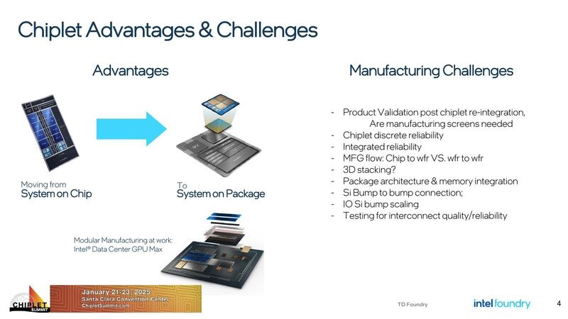
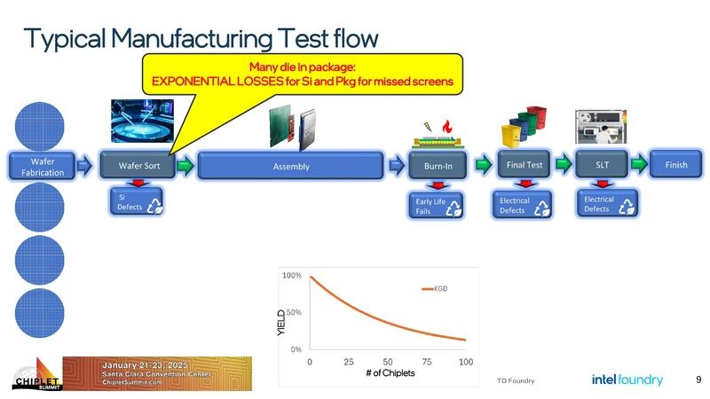
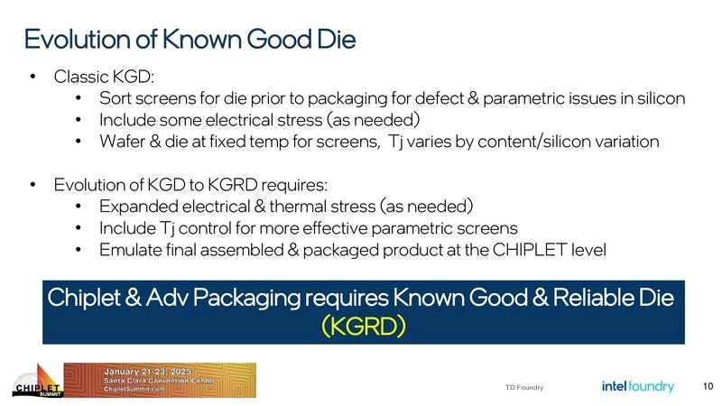
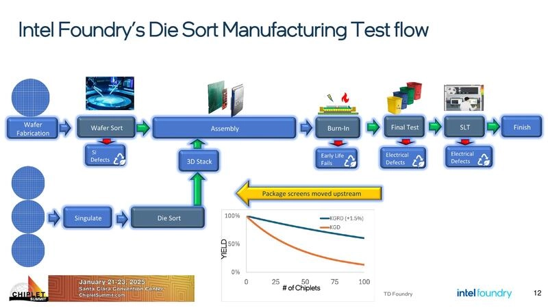
Advanced packaging is quickly becoming a key element in achieving the higher chip densities required by today’s AI/HPC applications. Large, complex packages containing multiple dies plus interposers and silicon bridges are now commonplace. However, the process of integrating chiplets and creating complex die stacks using technologies such as EMIB or Foveros is expensive and time-consuming. So it is essential to determine whether all the dies involved are good as early as possible. Fabs must spend more time and effort on sorting which screens chiplets upstream in the manufacturing flow. A promising approach uses advanced thermal control systems and sorting die post singulation. These technologies can make stress application and chiplet parametric determination more effective, enabling reliability and performance binning of dies. Better binning, in turn, can mean higher capture or attach rates of die to complex packages. The early elimination of chips with bad elements can save months in the early critical stages of manufacturing. Improved die sorts can lead the way to reducing overall cost, increasing yield, and shortening time-to-market of today's most complex and highest-performing chips.