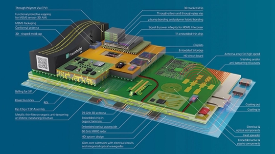
The APECS Pilot Line: Heterointegration enabling Chiplet Applications By Fraunhofer IZM March 13, 2025
The Future of Faster, Smaller, and More Efficient Chips: A Breakthrough in Hybrid Bonding By JoAnn Yamani March 3, 2025
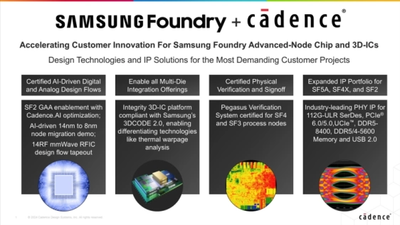
Cadence Recognized for Accelerating AI and 3D-IC Applications by Samsung Foundry By Cadence February 18, 2025
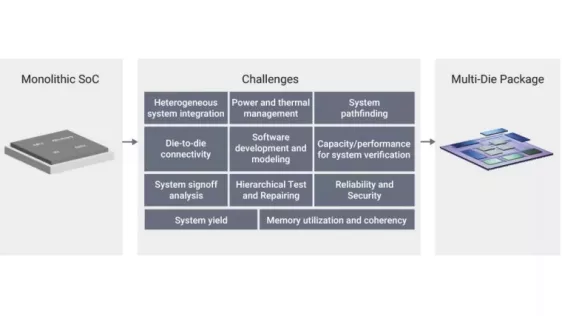
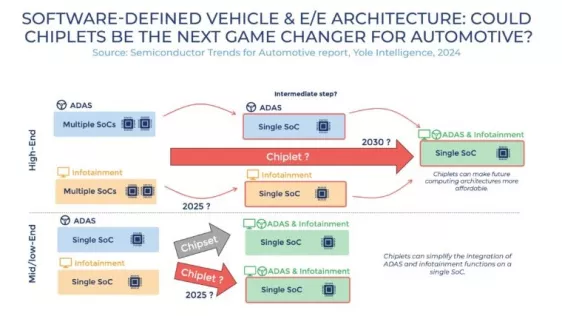
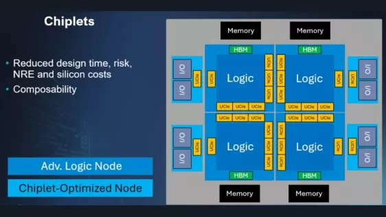
Embracing the Chiplet Journey: The Shift to Chiplet-Based Architectures By Kalar Rajendiran February 12, 2025
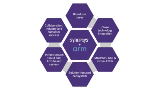
Synopsys Aims to Reduce Silicon Design Cycles by up to a Year in Collaboration with Arm By Arun Bhattacharya February 7, 2025
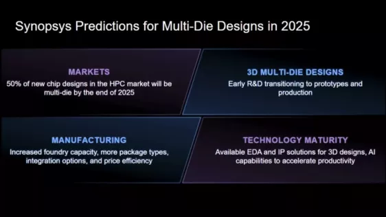
Synopsys Bold Prediction: 50% of New HPC Chip Designs Will Be Multi-Die in 2025 By Shekhar Kapoor, Michael Posner January 22, 2025
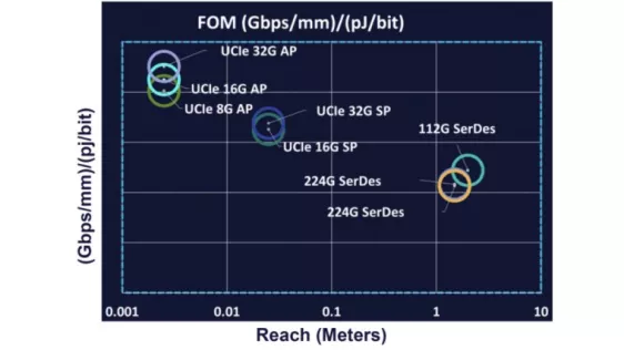
UCIe for 1.6T Interconnects in Next-Gen I/O Chiplets for AI data centers By Alphawave Semi January 21, 2025
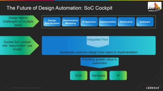
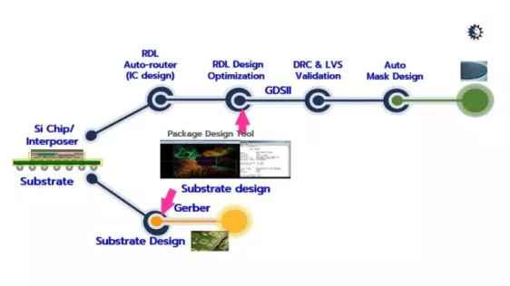
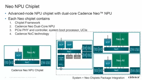
Integrated Design Ecosystem™ for Chiplets and Heterogeneous Integration in Advanced Packaging Technology By Dr. Lihong Cao, Sr. Director of Technology & Business Development January 21, 2025
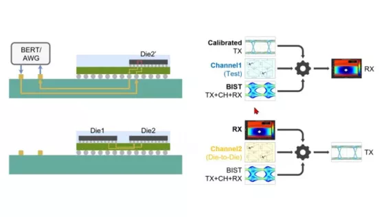
Multi-Die Health and Reliability: Synopsys and TSMC Showcase UCIe Advances By Faisal Goriawalla, Yervant Zorian January 10, 2025
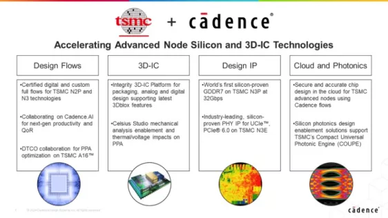
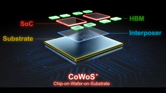
Cadence Collaborates with TSMC to Shape the Future of 3D-IC By Cadence Design Systems January 9, 2025
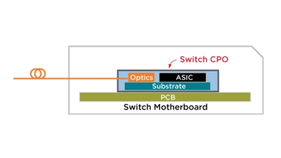
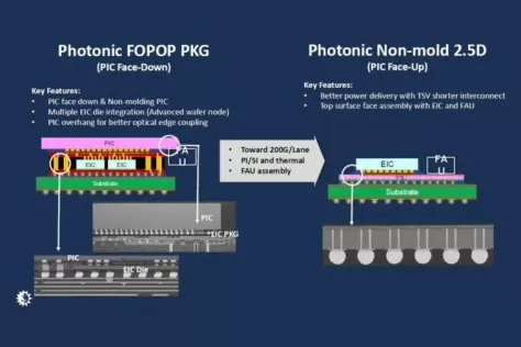
Advanced Packaging Evolution: Chiplet and Silicon Photonics-CPO By Vincent Lin - Director, Corporate R&D (ASE) January 8, 2025
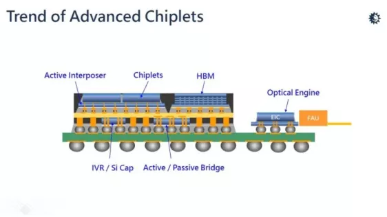
Unleashing AI Potential Through Advanced Chiplet Architectures By Tony Chan Carusone, CTO, Alphawave Semi December 11, 2024